SLUSDA9C may   2018  – august 2023 LV3842

PRODUCTION DATA  

  1.   1
  2. Features
  3. Applications
  4. Description
  5. Revision History
  6. Device Comparison Table
  7. Pin Configuration and Functions
  8. Specifications
    1. 7.1 Absolute Maximum Ratings
    2. 7.2 ESD Ratings
    3. 7.3 Recommended Operating Conditions
    4. 7.4 Thermal Information
    5. 7.5 Electrical Characteristics
    6. 7.6 Timing Requirements
    7. 7.7 Switching Characteristics
    8. 7.8 Typical Characteristics
  9. Detailed Description
    1. 8.1 Overview
    2. 8.2 Functional Block Diagram
    3. 8.3 Feature Description
      1. 8.3.1 Fixed Frequency Peak Current Mode Control
      2. 8.3.2 Adjustable Output Voltage
      3. 8.3.3 Enable
      4. 8.3.4 Minimum ON-Time, Minimum OFF-Time and Frequency Foldback
      5. 8.3.5 Bootstrap Voltage
      6. 8.3.6 Overcurrent and Short-Circuit Protection
      7. 8.3.7 Soft Start
      8. 8.3.8 Thermal Shutdown
    4. 8.4 Device Functional Modes
      1. 8.4.1 Shutdown Mode
      2. 8.4.2 Active Mode
      3. 8.4.3 CCM Mode
      4. 8.4.4 Light-Load Operation (PFM Version)
      5. 8.4.5 Light-Load Operation (FPWM Version)
  10. Application and Implementation
    1. 9.1 Application Information
    2. 9.2 Typical Application
      1. 9.2.1 Design Requirements
      2. 9.2.2 Detailed Design Procedure
        1. 9.2.2.1 Output Voltage Set-Point
        2. 9.2.2.2 Inductor Selection
        3. 9.2.2.3 Output Capacitor Selection
        4. 9.2.2.4 Input Capacitor Selection
        5. 9.2.2.5 Bootstrap Capacitor
        6. 9.2.2.6 Undervoltage Lockout Set-Point
      3. 9.2.3 Application Curves
    3. 9.3 Power Supply Recommendations
    4. 9.4 Layout
      1. 9.4.1 Layout Guidelines
      2. 9.4.2 Compact Layout for EMI Reduction
      3. 9.4.3 Feedback Resistors
      4. 9.4.4 Layout Example
  11. 10Device and Documentation Support
    1. 10.1 Documentation Support
      1. 10.1.1 Related Documentation
    2. 10.2 Receiving Notification of Documentation Updates
    3. 10.3 Support Resources
    4. 10.4 Trademarks
    5. 10.5 Electrostatic Discharge Caution
    6. 10.6 Glossary
  12. 11Mechanical, Packaging, and Orderable Information

Package Options

Mechanical Data (Package|Pins)
Thermal pad, mechanical data (Package|Pins)
Orderable Information

Description

The LV3842 is an easy to use synchronous step-down DC-DC converter capable of driving up to 600-mA load current. With a wide input range of 4 V to 36 V, the device is designed for a wide range of industrial applications for power conditioning from an unregulated source.

The LV3842 employs 1.1-MHz switching frequency for small solution size. The LV3842 also has FPWM (forced PWM) version to achieve constant frequency and small output voltage ripple over the full load range. Soft-start and compensation circuits are employed internally which allows the device to be used with minimum external components.

The device has built-in protection features, such as cycle-by-cycle current limit, hiccup mode short-circuit protection, and thermal shutdown in case of excessive power dissipation. The LV3842 is available in SOT-23-6 package.
Package Information
PART NUMBER PACKAGE(1) PACKAGE SIZE(2)
LV3842 DBV (SOT-23, 6) 2.90 mm × 2.80 mm
For all available packages, see the orderable addendum at the end of the data sheet.
The package size (length × width) is a nominal value and includes pins, where applicable.
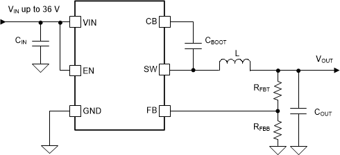
GUID-64797D28-4571-48FF-B26B-2653824222FD-low.gifTypical Application Schematic
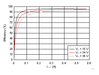
GUID-57FB82E4-47F2-41F2-A092-FB2E387C834A-low.gifEfficiency vs Output Current VOUT = 12 V, 1.1 MHz, FPWM