SLUSDA9C may   2018  – august 2023 LV3842

PRODUCTION DATA  

  1.   1
  2. Features
  3. Applications
  4. Description
  5. Revision History
  6. Device Comparison Table
  7. Pin Configuration and Functions
  8. Specifications
    1. 7.1 Absolute Maximum Ratings
    2. 7.2 ESD Ratings
    3. 7.3 Recommended Operating Conditions
    4. 7.4 Thermal Information
    5. 7.5 Electrical Characteristics
    6. 7.6 Timing Requirements
    7. 7.7 Switching Characteristics
    8. 7.8 Typical Characteristics
  9. Detailed Description
    1. 8.1 Overview
    2. 8.2 Functional Block Diagram
    3. 8.3 Feature Description
      1. 8.3.1 Fixed Frequency Peak Current Mode Control
      2. 8.3.2 Adjustable Output Voltage
      3. 8.3.3 Enable
      4. 8.3.4 Minimum ON-Time, Minimum OFF-Time and Frequency Foldback
      5. 8.3.5 Bootstrap Voltage
      6. 8.3.6 Overcurrent and Short-Circuit Protection
      7. 8.3.7 Soft Start
      8. 8.3.8 Thermal Shutdown
    4. 8.4 Device Functional Modes
      1. 8.4.1 Shutdown Mode
      2. 8.4.2 Active Mode
      3. 8.4.3 CCM Mode
      4. 8.4.4 Light-Load Operation (PFM Version)
      5. 8.4.5 Light-Load Operation (FPWM Version)
  10. Application and Implementation
    1. 9.1 Application Information
    2. 9.2 Typical Application
      1. 9.2.1 Design Requirements
      2. 9.2.2 Detailed Design Procedure
        1. 9.2.2.1 Output Voltage Set-Point
        2. 9.2.2.2 Inductor Selection
        3. 9.2.2.3 Output Capacitor Selection
        4. 9.2.2.4 Input Capacitor Selection
        5. 9.2.2.5 Bootstrap Capacitor
        6. 9.2.2.6 Undervoltage Lockout Set-Point
      3. 9.2.3 Application Curves
    3. 9.3 Power Supply Recommendations
    4. 9.4 Layout
      1. 9.4.1 Layout Guidelines
      2. 9.4.2 Compact Layout for EMI Reduction
      3. 9.4.3 Feedback Resistors
      4. 9.4.4 Layout Example
  11. 10Device and Documentation Support
    1. 10.1 Documentation Support
      1. 10.1.1 Related Documentation
    2. 10.2 Receiving Notification of Documentation Updates
    3. 10.3 Support Resources
    4. 10.4 Trademarks
    5. 10.5 Electrostatic Discharge Caution
    6. 10.6 Glossary
  12. 11Mechanical, Packaging, and Orderable Information

Package Options

Mechanical Data (Package|Pins)
Thermal pad, mechanical data (Package|Pins)
Orderable Information

Output Voltage Set-Point

The output voltage of the LV3842 device is externally adjustable using a resistor divider network. The divider network is comprised of top feedback resistor RFBT and bottom feedback resistor RFBB. Equation 7 is used to determine the output voltage of the converter:

Equation 7. GUID-14ED2DBD-7AA6-457A-8CE6-75F0DAAC1AAC-low.gif

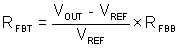
Choose the value of RFBB to be 22.1 kΩ. With the desired output voltage set to 5 V and the VREF = 1.0 V, the RFBT value can then be calculated using Equation 7. The formula yields to a value 88.4 kΩ, a standard value of 88.7 kΩ is selected.