SLLS350Q April 1999 – August 2024 MAX3243
PRODUCTION DATA
- 1
- 1 Features
- 2 Applications
- 3 Description
- 4 Pin Configuration and Functions
-
5 Specifications
- 5.1 Absolute Maximum Ratings
- 5.2 ESD Ratings
- 5.3 Recommended Operating Conditions
- 5.4 Thermal Information
- 5.5 Electrical Characteristics –– Auto Power Down
- 5.6 Electrical Characteristics –– Driver
- 5.7 Electrical Characteristics –– Receiver
- 5.8 Switching Characteristics –– Auto Power Down
- 5.9 Switching Characteristics –– Driver
- 5.10 Switching Characteristics –– Receiver
- 5.11 Typical Characteristics
- 6 Parameter Measurement Information
- 7 Detailed Description
- 8 Application and Implementation
- 9 Device and Documentation Support
- 10Revision History
- 11Mechanical, Packaging, and Orderable Information
Package Options
Mechanical Data (Package|Pins)
Thermal pad, mechanical data (Package|Pins)
- DW|28
Orderable Information
3 Description
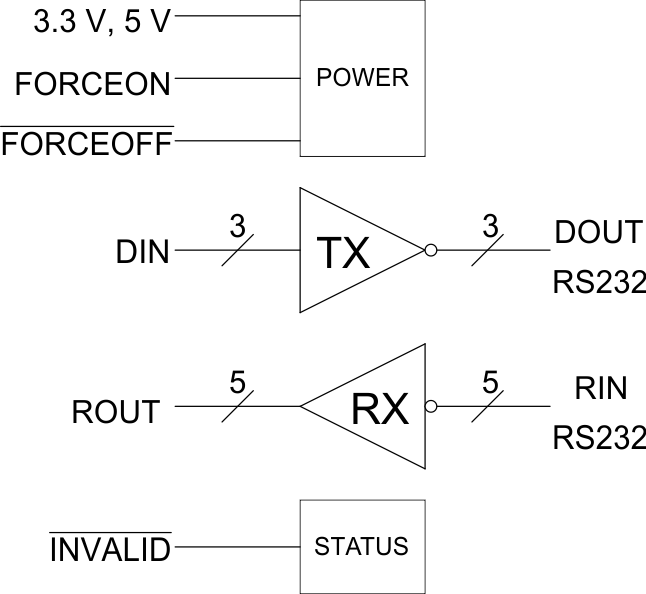
The MAX3243 device consists of three line drivers, five line receivers which is ideal for DE-9 DTE interface. ±15kV ESD (HBM) protection pin to pin (serial- port connection pins, including GND). Flexible power features saves power automatically. Special outputs ROUT2B and INVALID are always enabled to allow checking for ring indicator and valid RS232 input.
Package
Information
| PART NUMBER | PACKAGE(1) | PACKAGE SIZE(2) |
|---|---|---|
| MAX3243 | SSOP (28) | 10.2mm × 7.8mm |
| SOIC (28) | 17.9mm × 10.3mm | |
| TSSOP (28) | 9.7mm × 6.4mm |
(1) For more information, see Section 11.
(2) The package size (length × width) is a
nominal value and includes pins, where applicable.
 Simplified
Diagram