SLASE45E October 2014 – December 2019 MSP430FR2032 , MSP430FR2033
PRODUCTION DATA.
- 1Device Overview
- 2Revision History
- 3Device Comparison
- 4Terminal Configuration and Functions
-
5Specifications
- 5.1 Absolute Maximum Ratings
- 5.2 ESD Ratings
- 5.3 Recommended Operating Conditions
- 5.4 Active Mode Supply Current Into VCC Excluding External Current
- 5.5 Active Mode Supply Current Per MHz
- 5.6 Low-Power Mode LPM0 Supply Currents Into VCC Excluding External Current
- 5.7 Low-Power Mode LPM3 and LPM4 Supply Currents (Into VCC) Excluding External Current
- 5.8 Low-Power Mode LPMx.5 Supply Currents (Into VCC) Excluding External Current
- 5.9 Typical Characteristics, Low-Power Mode Supply Currents
- 5.10 Typical Characteristics - Current Consumption Per Module
- 5.11 Thermal Characteristics
- 5.12
Timing and Switching Characteristics
- 5.12.1 Power Supply Sequencing
- 5.12.2 Reset Timing
- 5.12.3 Clock Specifications
- 5.12.4 Digital I/Os
- 5.12.5 Timer_A
- 5.12.6
eUSCI
- Table 5-11 eUSCI (UART Mode) Recommended Operating Conditions
- Table 5-12 eUSCI (UART Mode) Switching Characteristics
- Table 5-13 eUSCI (SPI Master Mode) Recommended Operating Conditions
- Table 5-14 eUSCI (SPI Master Mode) Switching Characteristics
- Table 5-15 eUSCI (SPI Slave Mode) Switching Characteristics
- Table 5-16 eUSCI (I2C Mode) Switching Characteristics
- 5.12.7 ADC
- 5.12.8 FRAM
- 5.12.9 Emulation and Debug
-
6Detailed Description
- 6.1 CPU
- 6.2 Operating Modes
- 6.3 Interrupt Vector Addresses
- 6.4 Bootloader (BSL)
- 6.5 JTAG Standard Interface
- 6.6 Spy-Bi-Wire Interface (SBW)
- 6.7 FRAM
- 6.8 Memory Protection
- 6.9
Peripherals
- 6.9.1 Power Management Module (PMM) and On-chip Reference Voltages
- 6.9.2 Clock System (CS) and Clock Distribution
- 6.9.3 General-Purpose Input/Output Port (I/O)
- 6.9.4 Watchdog Timer (WDT)
- 6.9.5 System Module (SYS)
- 6.9.6 Cyclic Redundancy Check (CRC)
- 6.9.7 Enhanced Universal Serial Communication Interface (eUSCI_A0, eUSCI_B0)
- 6.9.8 Timers (Timer0_A3, Timer1_A3)
- 6.9.9 Real-Time Clock (RTC) Counter
- 6.9.10 10-Bit Analog Digital Converter (ADC)
- 6.9.11 Embedded Emulation Module (EEM)
- 6.9.12
Input/Output Diagrams
- 6.9.12.1 Port P1 Input/Output With Schmitt Trigger
- 6.9.12.2 Port P2 Input/Output With Schmitt Trigger
- 6.9.12.3 Port P3 Input/Output With Schmitt Trigger
- 6.9.12.4 Port P4.0 Input/Output With Schmitt Trigger
- 6.9.12.5 Port P4.1 and P4.2 Input/Output With Schmitt Trigger
- 6.9.12.6 Port 4.3, P4.4, P4.5, P4.6, and P4.7 Input/Output With Schmitt Trigger
- 6.9.12.7 Port P5.0, P5.1, P5.2, and P5.3 Input/Output With Schmitt Trigger
- 6.9.12.8 Port P5.4, P5.5, P5.6, and P5.7 Input/Output With Schmitt Trigger
- 6.9.12.9 Port P6.0, P6.1, P6.2, and P6.3 Input/Output With Schmitt Trigger
- 6.9.12.10 Port P6.4, P6.5, P6.6, and P6.7 Input/Output With Schmitt Trigger
- 6.9.12.11 Port P7.0, P7.1, P7.2, and P7.3 Input/Output With Schmitt Trigger
- 6.9.12.12 Port P7.4, P7.5, P7.6, and P7.7 Input/Output With Schmitt Trigger
- 6.9.12.13 Port P8.0 and P8.1 Input/Output With Schmitt Trigger
- 6.9.12.14 Port P8.2 and P8.3 Input/Output With Schmitt Trigger
- 6.10 Device Descriptors (TLV)
- 6.11 Memory
- 6.12 Identification
- 7Applications, Implementation, and Layout
- 8Device and Documentation Support
- 9Mechanical, Packaging, and Orderable Information
Package Options
Mechanical Data (Package|Pins)
Thermal pad, mechanical data (Package|Pins)
Orderable Information
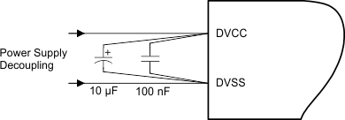
7.1.1 Power Supply Decoupling and Bulk Capacitors
TI recommends connecting a combination of a 10-µF plus a 100-nF low-ESR ceramic decoupling capacitor to the DVCC and DVSS pins. Higher-value capacitors may be used but can impact supply rail ramp-up time. Decoupling capacitors must be placed as close as possible to the pins that they decouple (within a few millimeters).
 Figure 7-1 Power Supply Decoupling