SLASE54D March 2016 – January 2021 MSP430FR5962 , MSP430FR5964 , MSP430FR5992 , MSP430FR5994 , MSP430FR59941
PRODUCTION DATA
- 1 Features
- 2 Applications
- 3 Description
- 4 Functional Block Diagram
- 5 Revision History
- 6 Device Comparison
- 7 Terminal Configuration and Functions
-
8 Specifications
- 8.1 Absolute Maximum Ratings
- 8.2 ESD Ratings
- 8.3 Recommended Operating Conditions
- 8.4 Active Mode Supply Current Into VCC Excluding External Current
- 8.5 Typical Characteristics, Active Mode Supply Currents
- 8.6 Low-Power Mode (LPM0, LPM1) Supply Currents Into VCC Excluding External Current
- 8.7 Low-Power Mode (LPM2, LPM3, LPM4) Supply Currents (Into VCC) Excluding External Current
- 8.8 Low-Power Mode (LPMx.5) Supply Currents (Into VCC) Excluding External Current
- 8.9 Typical Characteristics, Low-Power Mode Supply Currents
- 8.10 Typical Characteristics, Current Consumption per Module
- 8.11 Thermal Packaging Characteristics
- 8.12
Timing and Switching Characteristics
- 8.12.1 Power Supply Sequencing
- 8.12.2 Reset Timing
- 8.12.3 Clock Specifications
- 8.12.4 Wake-up Characteristics
- 8.12.5 Digital I/Os
- 8.12.6 LEA (Low-Energy Accelerator) (MSP430FR599x Only)
- 8.12.7 Timer_A and Timer_B
- 8.12.8 eUSCI
- 8.12.9
ADC12_B
- 8.12.9.1 12-Bit ADC, Power Supply and Input Range Conditions
- 8.12.9.2 12-Bit ADC, Timing Parameters
- 8.12.9.3 12-Bit ADC, Linearity Parameters
- 8.12.9.4 12-Bit ADC, Dynamic Performance With External Reference
- 8.12.9.5 12-Bit ADC, Dynamic Performance With Internal Reference
- 8.12.9.6 12-Bit ADC, Temperature Sensor and Built-In V1/2
- 8.12.9.7 12-Bit ADC, External Reference
- 8.12.10 Reference
- 8.12.11 Comparator
- 8.12.12 FRAM
- 8.12.13 Emulation and Debug
-
9 Detailed Description
- 9.1 Overview
- 9.2 CPU
- 9.3 Low-Energy Accelerator (LEA) for Signal Processing (MSP430FR599x Only)
- 9.4 Operating Modes
- 9.5 Interrupt Vector Table and Signatures
- 9.6 Bootloader (BSL)
- 9.7 JTAG Operation
- 9.8 FRAM Controller A (FRCTL_A)
- 9.9 RAM
- 9.10 Tiny RAM
- 9.11 Memory Protection Unit (MPU) Including IP Encapsulation
- 9.12
Peripherals
- 9.12.1 Digital I/O
- 9.12.2 Oscillator and Clock System (CS)
- 9.12.3 Power-Management Module (PMM)
- 9.12.4 Hardware Multiplier (MPY)
- 9.12.5 Real-Time Clock (RTC_C)
- 9.12.6 Watchdog Timer (WDT_A)
- 9.12.7 System Module (SYS)
- 9.12.8 DMA Controller
- 9.12.9 Enhanced Universal Serial Communication Interface (eUSCI)
- 9.12.10 TA0, TA1, and TA4
- 9.12.11 TA2 and TA3
- 9.12.12 TB0
- 9.12.13 ADC12_B
- 9.12.14 Comparator_E
- 9.12.15 CRC16
- 9.12.16 CRC32
- 9.12.17 AES256 Accelerator
- 9.12.18 True Random Seed
- 9.12.19 Shared Reference (REF)
- 9.12.20 Embedded Emulation
- 9.13
Input/Output Diagrams
- 9.13.1 Capacitive Touch Functionality on Ports P1 to P8, and PJ
- 9.13.2 Port P1 (P1.0 to P1.2) Input/Output With Schmitt Trigger
- 9.13.3 Port P1 (P1.3 to P1.5) Input/Output With Schmitt Trigger
- 9.13.4 Port P1 (P1.6 and P1.7) Input/Output With Schmitt Trigger
- 9.13.5 Port P2 (P2.0 to P2.2) Input/Output With Schmitt Trigger
- 9.13.6 Port P2 (P2.3 and P2.4) Input/Output With Schmitt Trigger
- 9.13.7 Port P2 (P2.5 and P2.6) Input/Output With Schmitt Trigger
- 9.13.8 Port P2 (P2.7) Input/Output With Schmitt Trigger
- 9.13.9 Port P3 (P3.0 to P3.3) Input/Output With Schmitt Trigger
- 9.13.10 Port P3 (P3.4 to P3.7) Input/Output With Schmitt Trigger
- 9.13.11 Port P4 (P4.0 to P4.3) Input/Output With Schmitt Trigger
- 9.13.12 Port P4 (P4.4 to P4.7) Input/Output With Schmitt Trigger
- 9.13.13 Port P5 (P5.0 to P5.7) Input/Output With Schmitt Trigger
- 9.13.14 Port P6 (P6.0 to P6.7) Input/Output With Schmitt Trigger
- 9.13.15 Port P7 (P7.0 to P7.3) Input/Output With Schmitt Trigger
- 9.13.16 Port P7 (P7.4 to P7.7) Input/Output With Schmitt Trigger
- 9.13.17 Port P8 (P8.0 to P8.3) Input/Output With Schmitt Trigger
- 9.13.18 Port PJ (PJ.4 and PJ.5) Input/Output With Schmitt Trigger
- 9.13.19 Port PJ (PJ.6 and PJ.7) Input/Output With Schmitt Trigger
- 9.13.20 Port PJ (PJ.0 to PJ.3) JTAG Pins TDO, TMS, TCK, TDI/TCLK, Input/Output With Schmitt Trigger
- 9.14 Device Descriptors (TLV)
- 9.15 Memory Map
- 9.16 Identification
- 10Applications, Implementation, and Layout
- 11Device and Documentation Support
- 12Mechanical, Packaging, and Orderable Information
Package Options
Mechanical Data (Package|Pins)
Thermal pad, mechanical data (Package|Pins)
- RGZ|48
Orderable Information
9.13.15 Port P7 (P7.0 to P7.3) Input/Output With Schmitt Trigger
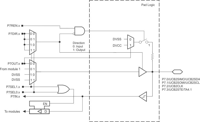
Figure 9-16 shows the port diagram. Table 9-33 summarizes the selection of the pin functions.

Functional representation only.
Figure 9-16 Port P7 (P7.0 to P7.3) DiagramTable 9-33 Port P7 (P7.0 to P7.3) Pin Functions
| PIN NAME (P7.x) | x | FUNCTION | CONTROL BITS AND SIGNALS (1) | ||
|---|---|---|---|---|---|
| P7DIR.x | P7SEL1.x | P7SEL0.x | |||
| P7.0/UCB2SIMO/UCB2SDA | 0 | P7.0 (I/O) | 0 = Input, 1 = Output | 0 | 0 |
| UCB2SIMO/UCB2SDA | X(2) | 0 | 1 | ||
| N/A | 0 | 1 | X | ||
| Internally tied to DVSS | 1 | ||||
| P7.1/UCB2SOMI/UCB2SCL | 1 | P7.1 (I/O) | 0 = Input, 1 = Output | 0 | 0 |
| UCB2SOMI/UCB2SCL | X(2) | 0 | 1 | ||
| N/A | 0 | 1 | X | ||
| Internally tied to DVSS | 1 | ||||
| P7.2/UCB2CLK | 2 | P7.2 (I/O) | 0 = Input, 1 = Output | 0 | 0 |
| UCB2CLK | X(2) | 0 | 1 | ||
| N/A | 0 | 1 | X | ||
| Internally tied to DVSS | 1 | ||||
| P7.3/UCB2STE/TA4.1 | 3 | P7.3 (I/O) | 0 = Input, 1 = Output | 0 | 0 |
| UCB2STE | X(2) | 0 | 1 | ||
| TA4.CCI1B | 0 | 1 | 0 | ||
| TA4.1 | 1 | ||||
| N/A | 0 | 1 | 1 | ||
| Internally tied to DVSS | 1 | ||||
(1) X = Don't care
(2) Direction controlled by eUSCI_B2 module.