NE5534x, SA5534x Low-Noise Operational Amplifiers
1 Features
- Equivalent Input Noise Voltage
3.5 nV/√Hz Typ - Unity-Gain Bandwidth 10 MHz Typ
- Common-Mode Rejection Ratio 100 dB Typ
- High DC Voltage Gain 100 V/mV Typ
- Peak-to-Peak Output Voltage Swing 32 V Typ With VCC± = ±18 V and RL = 600 Ω
- High Slew Rate 13 V/μs Typ
- Wide Supply-Voltage Range ±3 V to ±20 V
- Low Harmonic Distortion
- Offset Nulling Capability
- External Compensation Capability
2 Applications
- Audio Preamplifiers
- Servo Error Amplifiers
- Medical Equipment
- Telephone Channel Amplifiers
3 Description
The NE5534, NE5534A, SA5534, and SA5534A devices are high-performance operational amplifiers combining excellent dc and ac characteristics. Some of the features include very low noise, high output-drive capability, high unity-gain and maximum-output-swing bandwidths, low distortion, and high slew rate.
These operational amplifiers are compensated internally for a gain equal to or greater than three. Optimization of the frequency response for various applications can be obtained by use of an external compensation capacitor between COMP and COMP/BAL. The devices feature input-protection diodes, output short-circuit protection, and offset-voltage nulling capability with use of the BALANCE and COMP/BAL pins (see Figure 10).
For the NE5534A and SA5534A devices, a maximum limit is specified for the equivalent input noise voltage.
Device Information
| PART NUMBER | PACKAGE (PIN) | BODY SIZE (NOM) |
|---|---|---|
| NE5534x | SOIC (8) | 4.90 mm × 3.91 mm |
| SA5534x | SOIC (8) | 4.90 mm × 3.91 mm |
| SO (8) | 6.20 mm × 5.30 mm |
4 Simplified Schematic
5 Revision History
Changes from C Revision (September 2004) to D Revision
- Added Applications,Device Information table, Handling Ratings table, Feature Description section, Device Functional Modes, Application and Implementation section, Power Supply Recommendations section, Layout section, Device and Documentation Support section, and Mechanical, Packaging, and Orderable Information section.Go
- Deleted Ordering Information table.Go
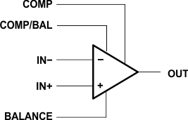
6 Pin Configuration and Functions

Pin Functions
| PIN | TYPE | DESCRIPTION | |
|---|---|---|---|
| NAME | NO. | ||
| BALANCE | 1 | I | External frequency compensation |
| COMP/BAL | 8 | I | External offset voltage adjustment/External frequency compensation |
| COMP | 5 | O | External offset voltage adjustment |
| IN+ | 3 | I | Noninverting input |
| IN- | 2 | I | Inverting Input |
| OUT | 6 | O | Output |
| VCC+ | 7 | — | Positive Supply |
| VCC- | 4 | — | Negative Supply |