SBOSA00B December 2019 – August 2020 OPA1637
PRODUCTION DATA
- 1 Features
- 2 Applications
- 3 Description
- 4 Revision History
- 5 Pin Configuration and Functions
- 6 Specifications
- 7 Parameter Measurement Information
- 8 Detailed Description
- 9 Application and Implementation
- 10Power Supply Recommendations
- 11Layout
- 12Device and Documentation Support
- 13Mechanical, Packaging, and Orderable Information
Package Options
Mechanical Data (Package|Pins)
- DGK|8
Thermal pad, mechanical data (Package|Pins)
Orderable Information
9.1.2 Operating the Power-Down Feature
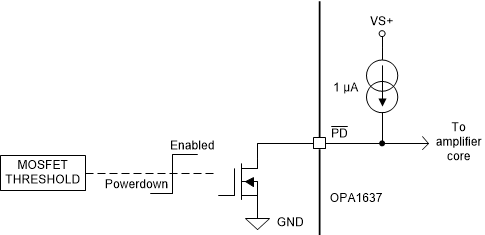
The power-down feature on the OPA1637 allows the device to be put into a low power-consumption state, in which quiescent current is minimized. To force the device into the low-power state, drive the PD pin lower than the power-down threshold voltage (VVS+ – 2 V). Driving the PD pin lower than the power-down threshold voltage forces the internal logic to disable both the differential and common-mode amplifiers. The PD pin has an internal pullup current that allows the pin to be used in an open-drain MOSFET configuration without an additional pullup resistor, as seen in Figure 9-2. In this configuration, the logic level can be referenced to the MOSFET, and the voltage at the PD pin is level-shifted to account for use with high supply voltages. Be sure to select an N-type MOSFET with a maximum BVDSS greater than the total supply voltage. For applications that do not use the power-down feature, tie the PD pin to the positive supply voltage.
 Figure 9-2 Power-Down (
PD) Pin Interface With Low-Voltage Logic Level Signals
Figure 9-2 Power-Down (
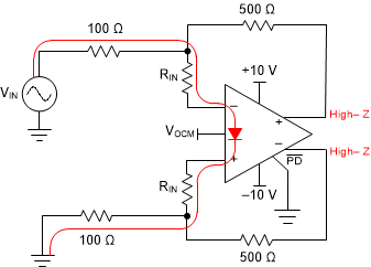
PD) Pin Interface With Low-Voltage Logic Level SignalsWhen PD is low (device is in power down) the output pins will be in a high-impedance state. When the device is in the power-down state, the outputs are high impedance, and the output voltage is no longer controlled by the amplifier, but dependant on the input and load configuration. In this case, the input voltage between IN– and IN+ can drift to a voltage that may forward-bias the input protection diodes. Take care to avoid high currents flowing through the input diodes by using an input resistor to limit the current to less than 10 mA. In Figure 9-3, the OPA1637 is configured in a differential gain of 5 with 100-Ω input resistors. When the device enters power down, the voltage between IN– and IN+ increases until the internal protection diode is forward-biased. In this case, exceeding a voltage on VIN with RIN= 0 Ω of 2.5 V (diode forward voltage estimated at 0.5 V) results in a current greater than 10 mA. To avoid this high current, select RIN so that the maximum current flow is less than 10 mA when VIN is at maximum voltage.
 Figure 9-3 Path of Input Current Flow When
PD = Low