SBOS058B December 1997 – November 2024 OPA134 , OPA2134 , OPA4134
PRODUCTION DATA
- 1
- 1 Features
- 2 Applications
- 3 Description
- 4 Pin Configuration and Functions
- 5 Specifications
- 6 Detailed Description
- 7 Application and Implementation
- 8 Device and Documentation Support
- 9 Revision History
- 10Mechanical, Packaging, and Orderable Information
Package Options
Refer to the PDF data sheet for device specific package drawings
Mechanical Data (Package|Pins)
- D|8
- P|8
Thermal pad, mechanical data (Package|Pins)
Orderable Information
6.2.2 Distortion Measurements
The distortion produced by OPAx134 series of operational amplifiers is below the measurement limit of all known commercially-available equipment. However, a special test circuit can extend the measurement capabilities.
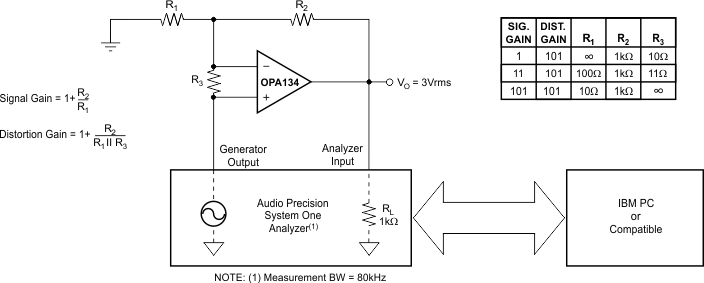
Operational amplifier distortion can be considered an internal error source which can be referred to the input. Figure 6-1 shows a circuit which causes the operational amplifier distortion to be 101 times greater than that which the operational amplifier normally produces. The addition of R3 to the otherwise standard non-inverting amplifier configuration alters the feedback factor or noise gain of the circuit. The closed-loop gain is unchanged, but the feedback available for error correction is reduced by a factor of 101, thus extending the resolution by 101. The input signal and load applied to the operational amplifier are the same as with conventional feedback without R3. Keep the value of R3 small to minimize effect on the distortion measurements.
 Figure 6-1 Distortion Test Circuit
This technique can be verified by duplicating measurements at high gain or high frequency, where the distortion is within the measurement capability of the test equipment. Measurements for this data sheet were made with an Audio Precision distortion and noise analyzer, which greatly simplifies repetitive measurements. The measurement technique can, however, be performed with manual distortion measurement instruments.