SBOS427F June 2017 – March 2021 OPA145 , OPA2145
PRODUCTION DATA
- 1 Features
- 2 Applications
- 3 Description
- 4 Revision History
- 5 Pin Configuration and Functions
- 6 Specifications
- 7 Detailed Description
- 8 Application and Implementation
- 9 Power Supply Recommendations
- 10Layout
- 11Device and Documentation Support
- 12Mechanical, Packaging, and Orderable Information
Package Options
Mechanical Data (Package|Pins)
Thermal pad, mechanical data (Package|Pins)
Orderable Information
7.3.7 EMI Rejection
The electromagnetic interference (EMI) rejection ratio, or EMIRR, describes the EMI immunity of operational amplifiers. An adverse effect that is common to many op amps is a change in the offset voltage as a result of RF signal rectification. An op amp that is more efficient at rejecting this change in offset as a result of EMI has a higher EMIRR and is quantified by a decibel value. Measuring EMIRR can be performed in many ways, but this section provides the EMIRR IN+, which specifically describes the EMIRR performance when the RF signal is applied to the noninverting input pin of the op amp. In general, only the noninverting input is tested for EMIRR for the following three reasons:
- Op amp input pins are known to be the most sensitive to EMI, and typically rectify RF signals better than the supply or output pins.
- The noninverting and inverting op amp inputs have symmetrical physical layouts and exhibit nearly matching EMIRR performance.
- EMIRR is easier to measure on noninverting pins than on other pins because the noninverting input terminal can be isolated on a PCB. This isolation allows the RF signal to be applied directly to the noninverting input terminal with no complex interactions from other components or connecting PCB traces.
The EMIRR IN+ of the OPAx145 is plotted versus frequency as shown in Figure 7-4. The OPAx145 unity-gain bandwidth is 5.5 MHz. EMIRR performance below this frequency denotes interfering signals that fall within the op amp bandwidth.See EMI Rejection Ratio of Operational Amplifiers, available for download from www.ti.com.
 Figure 7-4 OPAx145 EMIRR IN+
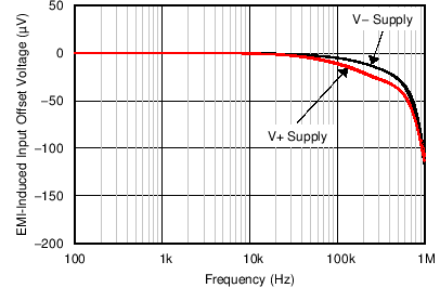
 Figure 7-5 OPAx145 EMI-Induced Input Offset Voltage
(Power Supplies)
Figure 7-5 OPAx145 EMI-Induced Input Offset Voltage
(Power Supplies)Table 7-1 lists the EMIRR IN+ values for the OPAx145 at particular frequencies commonly encountered in real-world applications. Applications listed in Table 7-1 may be centered on or operated near the particular frequency shown. This information may be of special interest to designers working with these types of applications, or working in other fields likely to encounter RF interference from broad sources, such as the industrial, scientific, and medical (ISM) radio band.
| FREQUENCY | APPLICATION OR ALLOCATION | EMIRR IN+ |
|---|---|---|
| 400 MHz | Mobile radio, mobile satellite, space operation, weather, radar, ultra-high frequency (UHF) applications | 54 dB |
| 900 MHz | Global system for mobile communications (GSM) applications, radio communication, navigation, GPS (to 1.6 GHz), GSM, aeronautical mobile, UHF applications | 68 dB |
| 1.8 GHz | GSM applications, mobile personal communications, broadband, satellite, L-band (1 GHz to 2 GHz) | 86 dB |
| 2.4 GHz | 802.11b, 802.11g, 802.11n, Bluetooth®, mobile personal communications, industrial, scientific and medical (ISM) radio band, amateur radio and satellite, S-band (2 GHz to 4 GHz) | 107 dB |
| 3.6 GHz | Radiolocation, aero communication and navigation, satellite, mobile, S-band | 100 dB |
| 5 GHz | 802.11a, 802.11n, aero communication and navigation, mobile communication, space and satellite operation, C-band (4 GHz to 8 GHz) | 105 dB |