SBOS309E August 2004 – December 2024 OPA2830
PRODUCTION DATA
- 1
- 1 Features
- 2 Applications
- 3 Description
- 4 Device Comparison Table
- 5 Pin Configurations and Functions
-
6 Specifications
- 6.1 Absolute Maximum Ratings
- 6.2 ESD Ratings
- 6.3 Recommended Operating Conditions
- 6.4 Thermal Information
- 6.5 Electrical Characteristics VS = ±5V
- 6.6 Electrical Characteristics VS = 5V
- 6.7 Electrical Characteristics VS = 3V
- 6.8 Typical Characteristics: VS = ±5V
- 6.9 Typical Characteristics: VS = ±5V, Differential Configuration
- 6.10 Typical Characteristics: VS = 5V
- 6.11 Typical Characteristics: VS = 5V, Differential Configuration
- 6.12 Typical Characteristics: VS = 3V
- 6.13 Typical Characteristics: VS = 3V, Differential Configuration
- 7 Parameter Measurement Information
-
8 Application and Implementation
- 8.1
Application Information
- 8.1.1 Wideband Voltage-Feedback Operation
- 8.1.2 Single-Supply ADC Interface
- 8.1.3 DC Level-Shifting
- 8.1.4 AC-Coupled Output Video Line Driver
- 8.1.5 Noninverting Amplifier With Reduced Peaking
- 8.1.6 Single-Supply Active Filter
- 8.1.7 Differential Low-Pass Active Filters
- 8.1.8 High-Pass Filters
- 8.1.9 High-Performance DAC Transimpedance Amplifier
- 8.1.10 Operating Suggestions Optimizing Resistor Values
- 8.1.11 Bandwidth vs Gain: Noninverting Operation
- 8.1.12 Inverting Amplifier Operation
- 8.1.13 Output Current and Voltages
- 8.1.14 Driving Capacitive Loads
- 8.1.15 Distortion Performance
- 8.1.16 Noise Performance
- 8.1.17 DC Accuracy and Offset Control
- 8.2 Power Supply Recommendations
- 8.3 Layout
- 8.1
Application Information
- 9 Device and Documentation Support
- 10Revision History
- 11Mechanical, Packaging, and Orderable Information
Package Options
Refer to the PDF data sheet for device specific package drawings
Mechanical Data (Package|Pins)
- D|8
- DGK|8
Thermal pad, mechanical data (Package|Pins)
Orderable Information
8.1.12 Inverting Amplifier Operation
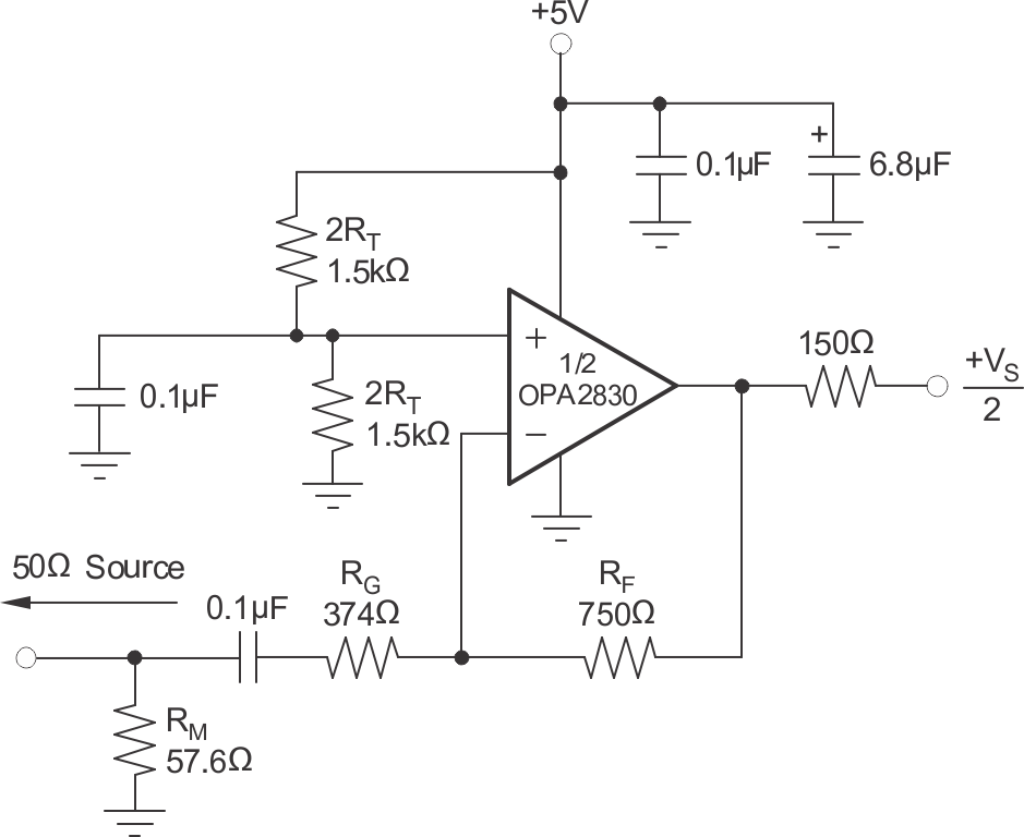
All of the familiar op amp application circuits are available to the designer with the OPA2830. Figure 8-15 shows a typical inverting configuration where the I/O impedance and signal gain from Figure 8-1 are retained in an inverting circuit configuration. Inverting operation is one of the more common requirements and offers several performance benefits. Inverting operation also allows the input to be biased at VS/2 without any headroom issues. The output voltage can be independently moved to be within the output voltage range with coupling capacitors or bias adjustment resistors.
 Figure 8-15 AC-Coupled, G = –2 Example Circuit
In the inverting configuration, consider three key design considerations. The first consideration is that the gain resistor (RG) becomes part of the signal channel input impedance. If input impedance matching is desired (which is beneficial whenever the signal is coupled through a cable, twisted pair, long PCB trace, or other transmission line conductor), RG can be set equal to the required termination value and RF adjusted to give the desired gain. This is the simplest approach and results in optimum bandwidth and noise performance.
However, at low inverting gains, the resulting feedback resistor value can present a significant load to the amplifier output. For an inverting gain of 2, setting RG to 50Ω for input matching eliminates the need for RM but requires a 100Ω feedback resistor. This configuration has the interesting advantage of the noise gain becoming equal to 2 for a 50Ω source impedance—the same as the noninverting circuits considered previously. The amplifier output now has the 100Ω feedback resistor in parallel with the external load. In general, the feedback resistor is limited to the 200Ω to 1.5kΩ range. In this case, preferably increase both the RF and RG values (see Figure 8-15), and then achieve the input matching impedance with a third resistor (RM) to ground. The total input impedance becomes the parallel combination of RG and RM.
The second major consideration, touched on in the previous paragraph, is that the signal source impedance becomes part of the noise gain equation and hence influences the bandwidth. For the example in Figure 8-15, the RM value combines in parallel with the external 50Ω source impedance (at high frequencies), yielding an effective driving impedance of 50Ω || 57.6Ω = 26.8Ω. This impedance is added in series with RG for calculating the noise gain. The resulting noise gain is 2.87 for Figure 8-15, as opposed to only 2 if RM can be eliminated as discussed above. The bandwidth can therefore be lower for the gain of –2 circuit of Figure 8-15 (NG = +2.87) than for the gain of +2 circuit of Figure 8-1.
The third important consideration in inverting amplifier design is setting the bias current cancellation resistors on the noninverting input (a parallel combination of RT = 750Ω). If this resistor is set equal to the total dc resistance looking out of the inverting node, the output dc error, due to the input bias currents, can be reduced to (input offset current) times RF. With the dc blocking capacitor in series with RG, the dc source impedance looking out of the inverting mode is simply RF = 750Ω for Figure 8-15. To reduce the additional high-frequency noise introduced by this resistor and power-supply feed-through, RT is bypassed with a capacitor.