SBOS771B December 2016 – November 2024 OPA4277-SP
PRODUCTION DATA
- 1
- 1 Features
- 2 Applications
- 3 Description
- 4 Pin Configuration and Functions
- 5 Specifications
- 6 Detailed Description
- 7 Application and Implementation
- 8 Device and Documentation Support
- 9 Revision History
- 10Mechanical, Packaging, and Orderable Information
Package Options
Refer to the PDF data sheet for device specific package drawings
Mechanical Data (Package|Pins)
- JDJ|28
- HFR|14
- KGD|0
Thermal pad, mechanical data (Package|Pins)
Orderable Information
6.3.2 Input Bias Current Cancellation
The input stage base current of the OPA4277-SP is internally compensated with an equal and opposite cancellation circuit. The resulting input bias current is the difference between the input stage base current and the cancellation current. This residual input bias current can be positive or negative.
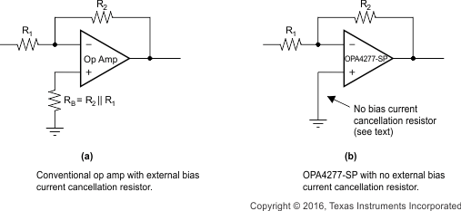
When the bias current is canceled in this manner, the input bias current and input offset current are approximately the same magnitude. As a result, using a bias current cancellation resistor is not necessary, as is often done with other operational amplifiers. Figure 6-2 (a) shows an op amp with an external bias current cancellation resistor and (b) shows the OPA4277-SP which requires no external bias current cancellation resistor. Be aware that a resistor added to cancel input bias current errors can actually increase offset voltage and noise.
 Figure 6-2 Input
Bias Current Cancellation