SBASA69A August   2023  – December 2023 OPT4003-Q1

PRODUCTION DATA  

  1.   1
  2. Features
  3. Applications
  4. Description
  5. Pin Configuration and Functions
  6. Specifications
    1. 5.1 Absolute Maximum Ratings
    2. 5.2 ESD Ratings
    3. 5.3 Recommended Operating Conditions
    4. 5.4 Thermal Information
    5. 5.5 Electrical Characteristics
    6. 5.6 Timing Requirements
    7. 5.7 Timing Diagram
    8. 5.8 Typical Characteristics
  7. Detailed Description
    1. 6.1 Overview
    2. 6.2 Functional Block Diagram
    3. 6.3 Feature Description
      1. 6.3.1 Spectral Response
        1. 6.3.1.1 Channel 0: Human Eye Matching
        2. 6.3.1.2 Channel 1: Near Infrared
      2. 6.3.2 Automatic Full-Scale Range Setting
      3. 6.3.3 Error Correction Code (ECC) Features
        1. 6.3.3.1 Output Sample Counter
        2. 6.3.3.2 Output CRC
        3. 6.3.3.3 Threshold Detection
    4. 6.4 Device Functional Modes
      1. 6.4.1 Modes of Operation
      2. 6.4.2 Interrupt Modes of Operation
      3. 6.4.3 Light Range Selection
      4. 6.4.4 Selecting Conversion Time
      5. 6.4.5 Light Measurement in Lux
      6. 6.4.6 Threshold Detection Calculations
      7. 6.4.7 Light Resolution
    5. 6.5 Programming
      1. 6.5.1 I2C Bus Overview
        1. 6.5.1.1 Serial Bus Address
        2. 6.5.1.2 Serial Interface
      2. 6.5.2 Writing and Reading
        1. 6.5.2.1 High-Speed I2C Mode
        2. 6.5.2.2 Burst Read Mode
        3. 6.5.2.3 General-Call Reset Command
        4. 6.5.2.4 SMBus Alert Response
  8. Register Maps
    1. 7.1 Register Descriptions
  9. Application and Implementation
    1. 8.1 Application Information
    2. 8.2 Typical Application
      1. 8.2.1 Electrical Interface
        1. 8.2.1.1 Design Requirements
          1. 8.2.1.1.1 Optical Interface
        2. 8.2.1.2 Detailed Design Procedure
          1. 8.2.1.2.1 Optomechanical Design
        3. 8.2.1.3 Application Curves
    3. 8.3 Best Design Practices
    4. 8.4 Power Supply Recommendations
    5. 8.5 Layout
      1. 8.5.1 Layout Guidelines
        1. 8.5.1.1 Soldering and Handling Recommendations
      2. 8.5.2 Layout Example
  10. Device and Documentation Support
    1. 9.1 Documentation Support
      1. 9.1.1 Related Documentation
    2. 9.2 Receiving Notification of Documentation Updates
    3. 9.3 Support Resources
    4. 9.4 Trademarks
    5. 9.5 Electrostatic Discharge Caution
    6. 9.6 Glossary
  11. 10Revision History
  12. 11Mechanical, Packaging, and Orderable Information

Package Options

Mechanical Data (Package|Pins)
Thermal pad, mechanical data (Package|Pins)
Orderable Information

Layout Guidelines

TI highly recommends placing the decoupling capacitor close to the device, but remember that optically reflective surfaces of components also affect the performance of the design. Consider the three-dimensional geometry of all components and structures around the sensor to prevent unexpected results from secondary optical reflections. Placing capacitors and components at a distance of at least twice the height of the component is usually sufficient. The best optical layout is to place all close components on the opposite side of the PCB from the OPT4003-Q1. However, this approach is not practical for the constraints of every design.

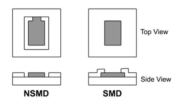
The device layout is also critical for good SMT assembly. Two types of land pattern pads can be used for this package: solder mask defined pads (SMD) and non-solder mask defined pads (NSMD). SMD pads have a solder mask opening that is smaller than the metal pads, whereas NSMD has a solder mask opening that is larger than the metal pad. Figure 8-3 illustrates these types of landing-pattern pads. SMD pads are preferred because these pads provide a more accurate soldering-pad dimension with the trace connections. For further discussion of SMT and PCB recommendations, see the Soldering and Handling Recommendations section.

GUID-014F4EA8-2DC8-4CA7-9D41-9CC73AD3C2F8-low.gif Figure 8-3 Solder Mask Defined Pad (SMD) and Non-Solder Mask Defined Pad (NSMD)