SBOSA84 December   2022 OPT4048

PRODUCTION DATA  

  1. Features
  2. Applications
  3. Description
  4. Revision History
  5. Description (continued)
  6. Pin Configuration and Functions
  7. Specifications
    1. 7.1 Absolute Maximum Ratings
    2. 7.2 ESD Ratings
    3. 7.3 Recommended Operating Conditions
    4. 7.4 Thermal Information
    5. 7.5 Electrical Characteristics
    6. 7.6 Typical Characteristics
  8. Detailed Description
    1. 8.1 Overview
    2. 8.2 Functional Block Diagram
    3. 8.3 Feature Description
      1. 8.3.1 Spectral Matching to CIE
      2. 8.3.2 Automatic Full-Scale Range Setting
      3. 8.3.3 Output Register CRC and Counter
        1. 8.3.3.1 Output Sample Counter
        2. 8.3.3.2 Output CRC
        3. 8.3.3.3 Threshold Detection
      4. 8.3.4 Device Functional Modes
        1. 8.3.4.1 Modes of Operation
        2. 8.3.4.2 Interrupt Modes of Operation
        3. 8.3.4.3 Light Range Selection
        4. 8.3.4.4 Selecting Conversion Time
        5. 8.3.4.5 Light and Color Measurement
        6. 8.3.4.6 Light Resolution
        7. 8.3.4.7 Programming
          1. 8.3.4.7.1 I2C Bus Overview
            1. 8.3.4.7.1.1 Serial Bus Address
            2. 8.3.4.7.1.2 Serial Interface
          2. 8.3.4.7.2 Writing and Reading
            1. 8.3.4.7.2.1 High-Speed I2C Mode
            2. 8.3.4.7.2.2 Burst Read Mode
            3. 8.3.4.7.2.3 General-Call Reset Command
            4. 8.3.4.7.2.4 SMBus Alert Response
    4. 8.4 Register Maps
      1. 8.4.1 ALL Register Map
  9. Application and Implementation
    1. 9.1 Application Information
    2. 9.2 Typical Application
      1. 9.2.1 Electrical Interface
      2. 9.2.2 Design Requirements
        1. 9.2.2.1 Optical Interface
      3. 9.2.3 Detailed Design Procedure
        1. 9.2.3.1 Optomechanical Design
      4. 9.2.4 Application Curves
    3. 9.3 Do's and Don'ts
    4. 9.4 Power Supply Recommendations
    5. 9.5 Layout
      1. 9.5.1 Layout Guidelines
      2. 9.5.2 Layout Example
      3. 9.5.3 Soldering and Handling Recommendations
  10. 10Device and Documentation Support
    1. 10.1 Documentation Support
      1. 10.1.1 Related Documentation
    2. 10.2 Receiving Notification of Documentation Updates
    3. 10.3 Support Resources
    4. 10.4 Trademarks
    5. 10.5 Electrostatic Discharge Caution
    6. 10.6 Glossary
  11. 11Mechanical, Packaging, and Orderable Information

Package Options

Mechanical Data (Package|Pins)
Thermal pad, mechanical data (Package|Pins)
Orderable Information

Soldering and Handling Recommendations

Soldering temperature profile and guidelines are published in future revisions of this document.

As with most optical devices, handle the OPT4048 with special care to ensure optical surfaces stay clean and free from damage. See Section 9.3 for more detailed recommendations. For best optical performance, solder flux and any other possible debris must be cleaned after soldering processes.
GUID-20221207-SS0I-RHKR-WPGK-K57XJ8WQRW2X-low.png
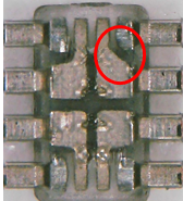
Note: The bottom side of the device features an angled feature to denote the PIN 1
Figure 9-6 Identification Feature for PIN 1
GUID-20221207-SS0I-LP23-2SFQ-FXD19RHSBWVS-low.png Figure 9-7 Identification Features for PIN 1 on Package