SCPS126G September   2006  – March 2021 PCA9538

PRODUCTION DATA  

  1. Features
  2. Description
  3. Revision History
  4. Pin Configuration and Functions
  5. Specifications
    1. 5.1 Absolute Maximum Ratings
    2. 5.2 ESD Ratings
    3. 5.3 Recommended Operating Conditions
    4. 5.4 Thermal Information
    5. 5.5 Electrical Characteristics
    6. 5.6 I2C Interface Timing Requirements
    7. 5.7 RESET Timing Requirements
    8. 5.8 Switching Characteristics
    9. 5.9 Typical Characteristics
  6. Parameter Measurement Information
  7. Detailed Description
    1. 7.1 Functional Block Diagram
    2. 7.2 Device Functional Modes
      1. 7.2.1 RESET Input
        1. 7.2.1.1 RESET Errata
          1.        System Impact
          2.        System Workaround
      2. 7.2.2 Power-On Reset
      3. 7.2.3 I/O Port
      4. 7.2.4 Interrupt Output ( INT)
        1. 7.2.4.1 Interrupt Errata
          1.        System Impact
          2.        System Workaround
    3. 7.3 Programming
      1. 7.3.1 I2C Interface
    4. 7.4 Register Maps
      1. 7.4.1 Device Address
      2. 7.4.2 Control Register And Command Byte
      3. 7.4.3 Register Descriptions
      4. 7.4.4 Bus Transactions
        1. 7.4.4.1 Writes
        2. 7.4.4.2 Reads
  8. Application Information Disclaimer
    1. 8.1 Application Information Disclaimer
    2. 8.2 Typical Application
      1. 8.2.1 Detailed Design Procedure
        1. 8.2.1.1 Minimizing ICC When I/Os Control Leds
  9. Power Supply Recommendations
    1. 9.1 Power-On Reset Requirements
  10. 10Device and Documentation Support
    1. 10.1 Receiving Notification of Documentation Updates
    2. 10.2 Support Resources
    3. 10.3 Trademarks
    4. 10.4 Electrostatic Discharge Caution
    5. 10.5 Glossary
  11. 11Mechanical, Packaging, and Orderable Information

Package Options

Mechanical Data (Package|Pins)
Thermal pad, mechanical data (Package|Pins)
Orderable Information

Device Address

Figure 7-6 shows the address byte of the PCA9538.
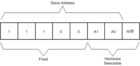
GUID-554B887E-9E9B-43C0-BAC5-AB92629C53D4-low.gifFigure 7-6 PCA9538 Address

Table 7-2 shows the PCA9538 address reference.

Table 7-2 Address Reference Table
INPUTSI2C BUS SLAVE ADDRESS
A1A0
LL112 (decimal), 70 (hexadecimal)
LH113 (decimal), 71 (hexadecimal)
HL114 (decimal), 72 (hexadecimal)
HH115 (decimal), 73 (hexadecimal)

The last bit of the slave address defines the operation (read or write) to be performed. When it is high (1), a read is selected while a low (0) selects a write operation.