SLASE64A December 2014 – June 2017 PCM1860-Q1 , PCM1861-Q1 , PCM1862-Q1 , PCM1863-Q1 , PCM1864-Q1 , PCM1865-Q1
PRODUCTION DATA.
- 1 Features
- 2 Applications
- 3 Description
- 4 Revision History
- 5 Device Comparison Table
- 6 Pin Configuration and Functions
-
7 Specifications
- 7.1 Absolute Maximum Ratings
- 7.2 ESD Ratings
- 7.3 Recommended Operating Conditions
- 7.4 Thermal Information
- 7.5 Electrical Characteristics: PGA and ADC AC Performance
- 7.6 Electrical Characteristics: DC
- 7.7 Electrical Characteristics: Digital Filter
- 7.8 Timing Requirements: External Clock
- 7.9 Timing Requirements: I2C Control Interface
- 7.10 Timing Requirements: SPI Control Interface
- 7.11 Timing Requirements: Audio Data Interface for Slave Mode
- 7.12 Timing Requirements: Audio Data Interface for Master Mode
- 7.13 Typical Characteristics
- 8 Parameter Measurement Information
-
9 Detailed Description
- 9.1 Overview
- 9.2 Functional Block Diagrams
- 9.3
Features Description
- 9.3.1 Analog Front End
- 9.3.2 Microphone Support
- 9.3.3 Input Multiplexer (PCM1860-Q1 and PCM1861-Q1)
- 9.3.4 Mixers and Multiplexers (PCM1862-Q1, PCM1863-Q1, PCM1864-Q1, and PCM1865-Q1)
- 9.3.5 Programmable Gain Amplifier
- 9.3.6 Automatic Clipping Suppression
- 9.3.7 Zero Crossing Detect
- 9.3.8 Digital Inputs
- 9.3.9
Clocks
- 9.3.9.1 Description
- 9.3.9.2 External Clock-Source Limits
- 9.3.9.3 Device Clock Distribution and Generation
- 9.3.9.4
Clocking Modes
- 9.3.9.4.1 Clock Configuration and Selection for Hardware-Controlled Devices
- 9.3.9.4.2 Clock Sources for Software-Controlled Devices
- 9.3.9.4.3 Clocking Configuration and Selection for Software-Controlled Devices
- 9.3.9.4.4 BCK Input Slave PLL Mode
- 9.3.9.4.5 Software-Controlled Devices ADC Non-Audio MCK PLL Mode
- 9.3.9.5 Software-Controlled Devices Manual PLL Calculation
- 9.3.9.6 Clock Halt and Error
- 9.3.9.7 Clock Halt and Error Detect
- 9.3.9.8 Changes in Clock Sources and Sample Rates
- 9.3.10 Analog-to-Digital Converters (ADCs)
- 9.3.11 Energysense
- 9.3.12 Audio Processing
- 9.3.13 Fade-In and Fade-Out Functions
- 9.3.14 Mappable GPIO Pins
- 9.3.15 Interrupt Controller
- 9.3.16 Audio Format Selection and Timing Details
- 9.4 Device Functional Modes
- 9.5 Programming
-
10Application and Implementation
- 10.1 Application Information
- 10.2 Typical Applications
- 11Power Supply Recommendations
- 12Layout
-
13Register Map
- 13.1 Register Map Description
- 13.2 Register Map Summary
- 13.3
Page 0 Registers
- 13.3.1 Page 0: Register 1 (address = 0x01) [reset = 0x00]
- 13.3.2 Page 0: Register 2 (address = 0x02) [reset = 0x00]
- 13.3.3 Page 0: Register 3 (address = 0x03) [reset = 0x00]
- 13.3.4 Page 0: Register 4 (address = 0x04) [reset = 0x00]
- 13.3.5 Page 0: Register 5 (address = 0x05) [reset = 0x86]
- 13.3.6 Page 0: Register 6 (address = 0x06) [reset = 0x41]
- 13.3.7 Page 0: Register 7 (address = 0x07) [reset = 0x41]
- 13.3.8 Page 0: Register 8 (address = 0x08) [reset = 0x42]
- 13.3.9 Page 0: Register 9 (address = 0x09) [reset = 0x42]
- 13.3.10 Page 0: Register 10 (address = 0x0A) [reset = 0x00]
- 13.3.11 Page 0: Register 11 (address = 0x0B) [reset = 0x44]
- 13.3.12 Page 0: Register 12 (address = 0x0C) [reset = 0x00]
- 13.3.13 Page 0: Register 13 (address = 0x0D) [reset = 0x00]
- 13.3.14 Page 0: Register 14 (address = 0x0E) [reset = 0x00]
- 13.3.15 Page 0: Register 15 (address = 0x0F) [reset = 0x00]
- 13.3.16 Page 0: Register 16 (address = 0x10) [reset = 0x01]
- 13.3.17 Page 0: Register 17 (address = 0x11) [reset = 0x20]
- 13.3.18 Page 0: Register 18 (address = 0x12) [reset = 0x00]
- 13.3.19 Page 0: Register 19 (address = 0x13) [reset = 0x00]
- 13.3.20 Page 0: Register 20 (address = 0x14) [reset = 0x00]
- 13.3.21 Page 0: Register 21 (address = 0x15) [reset = 0x00]
- 13.3.22 Page 0: Register 22 (address = 0x16) [reset = 0x00]
- 13.3.23 Page 0: Register 23 (address = 0x17) [reset = 0x00]
- 13.3.24 Page 0: Register 24 (address = 0x18) [reset = 0x00]
- 13.3.25 Page 0: Register 25 (address = 0x19) [reset = 0x00]
- 13.3.26 Page 0: Register 26 (address = 0x1A) [reset = 0x00]
- 13.3.27 Page 0: Register 27 (address = 0x1B) [reset = 0x00]
- 13.3.28 Page 0: Register 32 (address = 0x20) [reset = 0x01]
- 13.3.29 Page 0: Register 33 (address = 0x21) [reset = 0x00]
- 13.3.30 Page 0: Register 34 (address = 0x22) [reset = 0x01]
- 13.3.31 Page 0: Register 35 (address = 0x23) [reset = 0x03]
- 13.3.32 Page 0: Register 37 (address = 0x25) [reset = 0x07]
- 13.3.33 Page 0: Register 38 (address = 0x26) [reset = 0x03]
- 13.3.34 Page 0: Register 39 (address = 0x27) [reset = 0x3F]
- 13.3.35 Page 0: Register 40 (address = 0x28) [reset = 0x01]
- 13.3.36 Page 0: Register 41 (address = 0x29) [reset = 0x00]
- 13.3.37 Page 0: Register 42 (address = 0x2A) [reset = 0x00]
- 13.3.38 Page 0: Register 43 (address = 0x2B) [reset = 0x01]
- 13.3.39 Page 0: Register 44 (address = 0x2C) [reset = 0x00]
- 13.3.40 Page 0: Register 45 (address = 0x2D) [reset = 0x00]
- 13.3.41 Page 0: Register 48 (address = 0x30) [reset = 0x00]
- 13.3.42 Page 0: Register 49 (address = 0x31) [reset = 0x00]
- 13.3.43 Page 0: Register 50 (address = 0x32) [reset = 0x00]
- 13.3.44 Page 0: Register 51 (address = 0x33) [reset = 0x00]
- 13.3.45 Page 0: Register 52 (address = 0x34) [reset = 0x00]
- 13.3.46 Page 0: Register 54 (address = 0x36) [reset = 0x01]
- 13.3.47 Page 0: Register 64 (address = 0x40) [reset =0x80]
- 13.3.48 Page 0: Register 65 (address = 0x41) [reset = 0x7F]
- 13.3.49 Page 0: Register 66 (address = 0x42) [reset = 0x00]
- 13.3.50 Page 0: Register 67 (address = 0x43) [reset = 0x80]
- 13.3.51 Page 0: Register 68 (address = 0x44) [reset = 0x7F]
- 13.3.52 Page 0: Register 69 (address = 0x45) [reset = 0x00]
- 13.3.53 Page 0: Register 70 (address = 0x46) [reset = 0x80]
- 13.3.54 Page 0: Register 71 (address = 0x47) [reset = 0x7F]
- 13.3.55 Page 0: Register 72 (address = 0x48) [reset = 0x00]
- 13.3.56 Page 0: Register 73 (address = 0x49) [reset = 0x80]
- 13.3.57 Page 0: Register 74 (address = 0x4A) [reset = 0x7F]
- 13.3.58 Page 0: Register 75 (address = 0x4B) [reset = 0x00]
- 13.3.59 Page 0: Register 76 (address = 0x4C) [reset = 0x80]
- 13.3.60 Page 0: Register 77 (address = 0x4D) [reset = 0x7F]
- 13.3.61 Page 0: Register 78 (address = 0x4E) [reset = 0x00]
- 13.3.62 Page 0: Register 79 (address = 0x4F) [reset = 0x80]
- 13.3.63 Page 0: Register 80 (address = 0x50) [reset = 0x7F]
- 13.3.64 Page 0: Register 81 (address = 0x51) [reset = 0x00]
- 13.3.65 Page 0: Register 82 (address = 0x52) [reset = 0x80]
- 13.3.66 Page 0: Register 83 (address = 0x53) [reset = 0x7F]
- 13.3.67 Page 0: Register 84 (address = 0x54) [reset = 0x00]
- 13.3.68 Page 0: Register 85 (address = 0x55) [reset = 0x80]
- 13.3.69 Page 0: Register 86 (address = 0x56) [reset = 0x7F]
- 13.3.70 Page 0: Register 87 (address = 0x57) [reset = 0x00]
- 13.3.71 Page 0: Register 88 (address = 0x58) [reset = 0x00]
- 13.3.72 Page 0: Register 89 (address = 0x59) [reset = 0x00]
- 13.3.73 Page 0: Register 90 (address = 0x5A) [reset = 0x00]
- 13.3.74 Page 0: Register 96 (address = 0x60) [reset = 0x01]
- 13.3.75 Page 0: Register 97 (address = 0x61) [reset = 0x00]
- 13.3.76 Page 0: Register 98 (address = 0x62) [reset =0x10]
- 13.3.77 Page 0: Register 112 (address = 0x70) [reset = 0x70]
- 13.3.78 Page 0: Register 113 (address = 0x71) [reset = 0x10]
- 13.3.79 Page 0: Register 114 (address = 0x72) [reset = 0x00]
- 13.3.80 Page 0: Register 115 (address = 0x73) [reset = 0x00]
- 13.3.81 Page 0: Register 116 (address = 0x74) [reset = 0x00]
- 13.3.82 Page 0: Register 117 (address = 0x75) [reset = 0x00]
- 13.3.83 Page 0: Register 120 (address = 0x78) [reset = 0x00]
- 13.4
Page 1 Registers
- 13.4.1 Page 1: Register 1 (address = 0x01) [reset = 0x00]
- 13.4.2 Page 1: Register 2 (address = 0x02) [reset = 0x00]
- 13.4.3 Page 1: Register 4 (address = 0x04) [reset = 0x00]
- 13.4.4 Page 1: Register 5 (address = 0x05) [reset = 0x00]
- 13.4.5 Page 1: Register 6 (address = 0x06) [reset = 0x00]
- 13.4.6 Page 1: Register 7 (address = 0x07) [reset = 0x00]
- 13.4.7 Page 1: Register 8 (address = 0x08) [reset = 0x00]
- 13.4.8 Page 1: Register 9 (address = 0x09) [reset = 0x00]
- 13.4.9 Page 1: Register 10 (address = 0x0A) [reset = 0x00]
- 13.4.10 Page 1: Register 11 (address = 0x0B) [reset = 0x00]
- 13.5 Page 3 Registers
- 13.6 Page 253 Registers
- 14Device and Documentation Support
- 15Mechanical, Packaging, and Orderable Information
Package Options
Mechanical Data (Package|Pins)
- DBT|30
Thermal pad, mechanical data (Package|Pins)
Orderable Information
10 Application and Implementation
NOTE
Information in the following applications sections is not part of the TI component specification, and TI does not warrant its accuracy or completeness. TI’s customers are responsible for determining suitability of components for their purposes. Customers should validate and test their design implementation to confirm system functionality.
The PCM186x-Q1 family is extremely flexible, and this flexibility gives rise to a number of design questions that define the design requirements for a given application.
10.1 Application Information
In this section, the design choices are described, followed by a typical system implementation. The simplified application diagrams shown in Figure 64 and Figure 66 illustrate a typical system that would require the following architecture decisions to be made:
-
Device Control Method
- Hardware Control (PCM1860-Q1, PCM1861-Q1)
- Software Control (PCM1862-Q1, PCM1863-Q1, PCM1864-Q1 and PCM1865-Q1)
- SPI
- I2C
-
Power-Supply Options
- Single supply
- Separate analog and digital supplies
- Separate IO supply
-
Master Clock Source
- External CMOS-level clock
- External crystal with integrated oscillator
-
Analog Input Configuration
- Single-ended
- Differential
An example application diagram is shown in Figure 54.
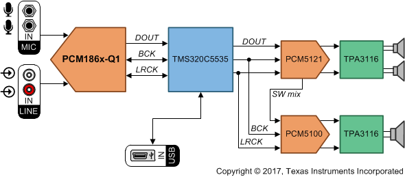 Figure 54. Example Application Diagram
10.1.1 Device Control Method
10.1.1.1 Hardware Control
The PCM1860-Q1 and PCM1861-Q1 are controlled with pullup or pulldown voltages on pins MD0 through MD6. The INT pin is ideally designed to be used with a microcontroller that can treat the pin as both an input (when used as an interrupt) and as an output to pull the pin high, and force power down. See the Pin Configuration and Functions for the PCM1860-Q1 and PCM1861-Q1 for specific configuration details. The hardware control interface is shown in Figure 55.
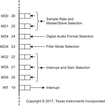 Figure 55. PCM1860-Q1 and PCM1861-Q1 Hardware Control Interface
10.1.1.2 Software Control
10.1.1.2.1 SPI Control
SPI control is selected by the MD0 pin; in this case, MDO connects to 3.3 V, so that the device acts as an SPI slave. The SPI control interface is shown in Figure 56.
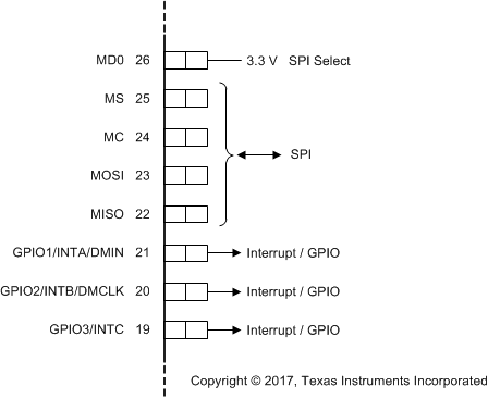 Figure 56. SPI Control Interface Including Interrupt Signals
10.1.1.2.2 I2C Control
I2C control is selected by the MD0 pin; in this example, MDO is pulled down to ground, so that the device acts as an I2C slave. One address line is supported to select between two devices on the same bus. The I2C control interface is shown in Figure 57.
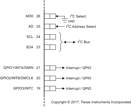 Figure 57. I2C Control Interface Including Interrupt Signals
10.1.2 Power-Supply Options
10.1.2.1 3.3-V AVDD, DVDD, and IOVDD
The 3.3-V AVDD, DVDD, and IOVDD Example is the most typical power-supply configuration. The 3.3-V single supply is shown in Figure 58.
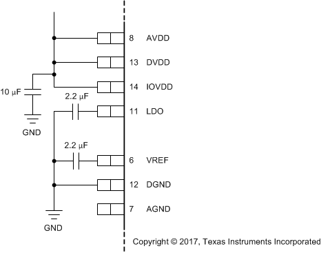 Figure 58. Single 3.3-V Supply
10.1.2.2 3.3-V AVDD, DVDD, and 1.8-V IOVDD
For details regarding lower-power applications, see 3.3-V AVDD, DVDD With 1.8-V IOVDD Example for Lower-Power Applications for lower-power applications.
10.1.3 Master Clock Source
The PCM186x-Q1 family offers three different clock sources. For the highest performance, run the ADC in master mode from a stable, well-known SCK source, such as a CMOS SCK, or a external crystal (XTAL). The PCM186x-Q1 is easy to hook up to a crystal, simply connect to XI and XO, and add capacitors to ground, as suggested in the XTAL manufacturer's data sheet (typically 15 pF).
External CMOS clock sources can be brought directly into the SCKI pin (for 3.3-V sources) or into the XI pin (1.8 V sources).
The PLL must be enabled if the clock source is unrelated to the audio rate. For instance, a 12-MHz USB crystal requires custom PLL settings to generate the 48-kHz rate clocks and the 44.1-kHz rate clocks required by many audio systems. An example with a 12-MHz clock is shown in Software-Controlled Devices Manual PLL Calculation.
For timing limits on XTAL and SCKI, see the Specifications section.
10.1.4 Dual PCM186x-Q1 TDM Functionality
Two PCM186x-Q1 software-controlled devices can be used together to create an 8-channel (or higher) channel count system using a TDM. In Figure 59, Device A is used as the TDM clock master, and Device B is configured to be a TDM slave and transmit on channels 5, 6, 7, and 8 of the TDM stream. The key difference is that Device A most likely has a crystal, or an SCKI source, and is configured to be the TDM master, whereas Device B does not require an XTAL or SCKI source because Device B uses the internal PLL to generate the required system clocks. Another two channels can be added to the stream from a stereo device; however, I2C address management is required because the PCM186x-Q1 software-controlled devices can only have one of two I2C addresses.
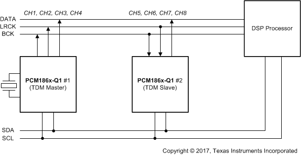 Figure 59. TDM With Two PCM186x-Q1
10.1.5 Analog Input Configuration
10.1.5.1 Analog Front-End Circuit For Single-Ended, Line-In Applications
Most systems can simply use an input filter similar to the one shown in Figure 60. However, for systems with significant out-of-band noise, a simple filter such as that shown in Figure 61 can be used for pre-ADC, antialiasing filtering. The recommended resistor value for the antialiasing filter is 100 Ω. Place film-type capacitors of 0.01 µF as close as possible to the VINLx and VINRx pins, and terminate to GND as close as possible to the AGND pin in order to maximize the dynamic performance of the ADC.
Adding this filter resistor also adds some input current limiting into the device, if the ESD diodes begin to clamp the signal when the maximum input voltage is exceeded. Keep the current through the input ESD diodes as low as possible, with ~5 mA treated as a absolute maximum. Any higher and the ESD diodes may fail because of the thermal constraints.
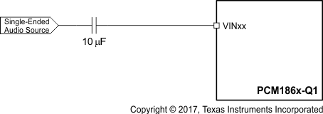 Figure 60. Analog Input Circuit for Single-Ended Input Applications
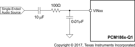 Figure 61. Analog Input Circuit With Additional Anti Aliasing Filter for Single-Ended Applications
10.1.5.2 Analog Front-End Circuit for Differential, Line-In Applications
As in single-ended applications, most systems can simply use an input filter similar to Figure 62. However, for systems with significant out-of-band noise, a simple filter such as that shown in Figure 63 can be used for pre-ADC, antialiasing filtering. The recommended resistor value for the antialiasing filter is 47 Ω. Place film-type capacitors of 0.01 µF as close as possible to the VINLx and VINRx pins, and terminate to GND as close as possible to the AGND pin in order to maximize the dynamic performance of ADC. To maintain common-mode rejection, match the series resistors as closely as possible.
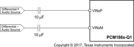 Figure 62. Analog Input Circuit for Differential Input Applications
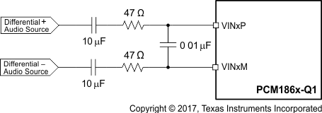 Figure 63. Differential Input Circuit With Additional AntiAliasing Filter
10.2 Typical Applications
10.2.1 Stereo Recording Application for PCM186x-Q1 Hardware-Controlled Devices in Master Mode
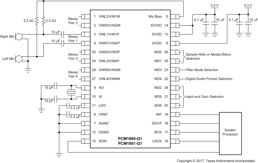
10.2.1.1 Design Requirements
- Device control method: Hardware control by digital GPIO pins of a microcontroller
- XTAL used for master mode
- Single-ended analog inputs
10.2.1.2 Detailed Design Procedure
- Device control method: Hardware control by digital GPIO pins of a microcontroller
- Select XTAL capacitors by reading the XTAL data sheet
- Single-ended analog inputs
- MD2, MD5, MD6 configuration (see the Pin Configuration and Functions for the PCM1860-Q1 and PCM1861-Q1)
- Audio slave mode
- MD0, MD1 grounded (see Figure 64, and the Pin Configuration and Functions for the PCM1860-Q1 and PCM1861-Q1)
- The power rails in this application allow the usage of X7R Ceramic capacitors. A maximum voltage rating of 6.3 V should be enough for the power supply capacitors.
- Configure the microcontroller INT pin to be an input for interrupts, or change the function to output to pull high to power down the PCM1860-Q1 and PCM1861-Q1.
10.2.1.3 Application Curves
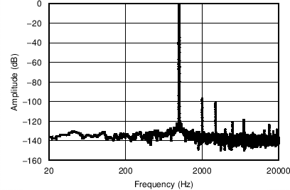 Figure 65. Frequency Response with –1-dB Input at 1 kHz
10.2.2 Stereo Recording Application for PCM186x-Q1 Software-Controlled Devices in Slave PLL Mode with 1.8-V IOVDD
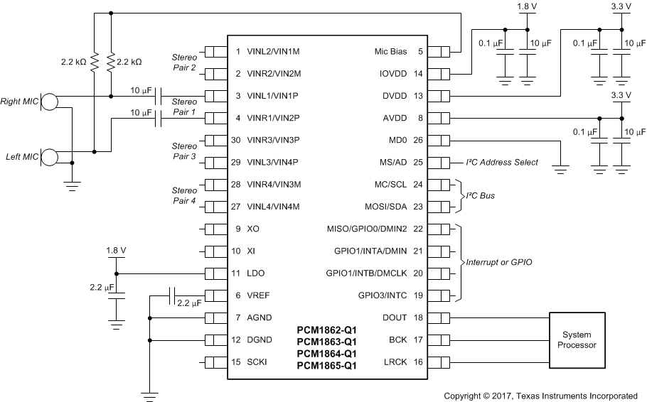
10.2.2.1 Design Requirements
- Device control method: Software control by I2C
- Clock slave to a 1.8-V device that only supplies BCK and LRCK (such as a Bluetooth module)
- Single-ended analog inputs
10.2.2.2 Detailed Design Procedure
- Device control method: Configure for I2C by pulling MD0 to GND, and setting I2C address by setting the AD pin high or low
- Make sure that BCK is configured in clock master device to be 64 × fS for automatic PLL setting to function.
- Single-ended analog inputs
- Audio slave mode
- Configure appropriate clock registers
- Page 0, 0x20 - Set MST_MODE = 1 (I2S slave)
- The power rails in this application allow the usage of X7R ceramic capacitors. A maximum voltage rating of 6.3 V should be enough for the power-supply capacitors.
10.2.2.3 Application Curves
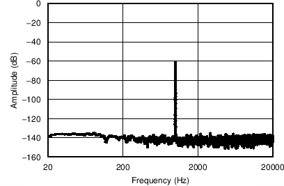 Figure 67. Frequency Response With –60-dB Input at 1 kHz