SLASE64A December 2014 – June 2017 PCM1860-Q1 , PCM1861-Q1 , PCM1862-Q1 , PCM1863-Q1 , PCM1864-Q1 , PCM1865-Q1
PRODUCTION DATA.
- 1 Features
- 2 Applications
- 3 Description
- 4 Revision History
- 5 Device Comparison Table
- 6 Pin Configuration and Functions
-
7 Specifications
- 7.1 Absolute Maximum Ratings
- 7.2 ESD Ratings
- 7.3 Recommended Operating Conditions
- 7.4 Thermal Information
- 7.5 Electrical Characteristics: PGA and ADC AC Performance
- 7.6 Electrical Characteristics: DC
- 7.7 Electrical Characteristics: Digital Filter
- 7.8 Timing Requirements: External Clock
- 7.9 Timing Requirements: I2C Control Interface
- 7.10 Timing Requirements: SPI Control Interface
- 7.11 Timing Requirements: Audio Data Interface for Slave Mode
- 7.12 Timing Requirements: Audio Data Interface for Master Mode
- 7.13 Typical Characteristics
- 8 Parameter Measurement Information
-
9 Detailed Description
- 9.1 Overview
- 9.2 Functional Block Diagrams
- 9.3
Features Description
- 9.3.1 Analog Front End
- 9.3.2 Microphone Support
- 9.3.3 Input Multiplexer (PCM1860-Q1 and PCM1861-Q1)
- 9.3.4 Mixers and Multiplexers (PCM1862-Q1, PCM1863-Q1, PCM1864-Q1, and PCM1865-Q1)
- 9.3.5 Programmable Gain Amplifier
- 9.3.6 Automatic Clipping Suppression
- 9.3.7 Zero Crossing Detect
- 9.3.8 Digital Inputs
- 9.3.9
Clocks
- 9.3.9.1 Description
- 9.3.9.2 External Clock-Source Limits
- 9.3.9.3 Device Clock Distribution and Generation
- 9.3.9.4
Clocking Modes
- 9.3.9.4.1 Clock Configuration and Selection for Hardware-Controlled Devices
- 9.3.9.4.2 Clock Sources for Software-Controlled Devices
- 9.3.9.4.3 Clocking Configuration and Selection for Software-Controlled Devices
- 9.3.9.4.4 BCK Input Slave PLL Mode
- 9.3.9.4.5 Software-Controlled Devices ADC Non-Audio MCK PLL Mode
- 9.3.9.5 Software-Controlled Devices Manual PLL Calculation
- 9.3.9.6 Clock Halt and Error
- 9.3.9.7 Clock Halt and Error Detect
- 9.3.9.8 Changes in Clock Sources and Sample Rates
- 9.3.10 Analog-to-Digital Converters (ADCs)
- 9.3.11 Energysense
- 9.3.12 Audio Processing
- 9.3.13 Fade-In and Fade-Out Functions
- 9.3.14 Mappable GPIO Pins
- 9.3.15 Interrupt Controller
- 9.3.16 Audio Format Selection and Timing Details
- 9.4 Device Functional Modes
- 9.5 Programming
-
10Application and Implementation
- 10.1 Application Information
- 10.2 Typical Applications
- 11Power Supply Recommendations
- 12Layout
-
13Register Map
- 13.1 Register Map Description
- 13.2 Register Map Summary
- 13.3
Page 0 Registers
- 13.3.1 Page 0: Register 1 (address = 0x01) [reset = 0x00]
- 13.3.2 Page 0: Register 2 (address = 0x02) [reset = 0x00]
- 13.3.3 Page 0: Register 3 (address = 0x03) [reset = 0x00]
- 13.3.4 Page 0: Register 4 (address = 0x04) [reset = 0x00]
- 13.3.5 Page 0: Register 5 (address = 0x05) [reset = 0x86]
- 13.3.6 Page 0: Register 6 (address = 0x06) [reset = 0x41]
- 13.3.7 Page 0: Register 7 (address = 0x07) [reset = 0x41]
- 13.3.8 Page 0: Register 8 (address = 0x08) [reset = 0x42]
- 13.3.9 Page 0: Register 9 (address = 0x09) [reset = 0x42]
- 13.3.10 Page 0: Register 10 (address = 0x0A) [reset = 0x00]
- 13.3.11 Page 0: Register 11 (address = 0x0B) [reset = 0x44]
- 13.3.12 Page 0: Register 12 (address = 0x0C) [reset = 0x00]
- 13.3.13 Page 0: Register 13 (address = 0x0D) [reset = 0x00]
- 13.3.14 Page 0: Register 14 (address = 0x0E) [reset = 0x00]
- 13.3.15 Page 0: Register 15 (address = 0x0F) [reset = 0x00]
- 13.3.16 Page 0: Register 16 (address = 0x10) [reset = 0x01]
- 13.3.17 Page 0: Register 17 (address = 0x11) [reset = 0x20]
- 13.3.18 Page 0: Register 18 (address = 0x12) [reset = 0x00]
- 13.3.19 Page 0: Register 19 (address = 0x13) [reset = 0x00]
- 13.3.20 Page 0: Register 20 (address = 0x14) [reset = 0x00]
- 13.3.21 Page 0: Register 21 (address = 0x15) [reset = 0x00]
- 13.3.22 Page 0: Register 22 (address = 0x16) [reset = 0x00]
- 13.3.23 Page 0: Register 23 (address = 0x17) [reset = 0x00]
- 13.3.24 Page 0: Register 24 (address = 0x18) [reset = 0x00]
- 13.3.25 Page 0: Register 25 (address = 0x19) [reset = 0x00]
- 13.3.26 Page 0: Register 26 (address = 0x1A) [reset = 0x00]
- 13.3.27 Page 0: Register 27 (address = 0x1B) [reset = 0x00]
- 13.3.28 Page 0: Register 32 (address = 0x20) [reset = 0x01]
- 13.3.29 Page 0: Register 33 (address = 0x21) [reset = 0x00]
- 13.3.30 Page 0: Register 34 (address = 0x22) [reset = 0x01]
- 13.3.31 Page 0: Register 35 (address = 0x23) [reset = 0x03]
- 13.3.32 Page 0: Register 37 (address = 0x25) [reset = 0x07]
- 13.3.33 Page 0: Register 38 (address = 0x26) [reset = 0x03]
- 13.3.34 Page 0: Register 39 (address = 0x27) [reset = 0x3F]
- 13.3.35 Page 0: Register 40 (address = 0x28) [reset = 0x01]
- 13.3.36 Page 0: Register 41 (address = 0x29) [reset = 0x00]
- 13.3.37 Page 0: Register 42 (address = 0x2A) [reset = 0x00]
- 13.3.38 Page 0: Register 43 (address = 0x2B) [reset = 0x01]
- 13.3.39 Page 0: Register 44 (address = 0x2C) [reset = 0x00]
- 13.3.40 Page 0: Register 45 (address = 0x2D) [reset = 0x00]
- 13.3.41 Page 0: Register 48 (address = 0x30) [reset = 0x00]
- 13.3.42 Page 0: Register 49 (address = 0x31) [reset = 0x00]
- 13.3.43 Page 0: Register 50 (address = 0x32) [reset = 0x00]
- 13.3.44 Page 0: Register 51 (address = 0x33) [reset = 0x00]
- 13.3.45 Page 0: Register 52 (address = 0x34) [reset = 0x00]
- 13.3.46 Page 0: Register 54 (address = 0x36) [reset = 0x01]
- 13.3.47 Page 0: Register 64 (address = 0x40) [reset =0x80]
- 13.3.48 Page 0: Register 65 (address = 0x41) [reset = 0x7F]
- 13.3.49 Page 0: Register 66 (address = 0x42) [reset = 0x00]
- 13.3.50 Page 0: Register 67 (address = 0x43) [reset = 0x80]
- 13.3.51 Page 0: Register 68 (address = 0x44) [reset = 0x7F]
- 13.3.52 Page 0: Register 69 (address = 0x45) [reset = 0x00]
- 13.3.53 Page 0: Register 70 (address = 0x46) [reset = 0x80]
- 13.3.54 Page 0: Register 71 (address = 0x47) [reset = 0x7F]
- 13.3.55 Page 0: Register 72 (address = 0x48) [reset = 0x00]
- 13.3.56 Page 0: Register 73 (address = 0x49) [reset = 0x80]
- 13.3.57 Page 0: Register 74 (address = 0x4A) [reset = 0x7F]
- 13.3.58 Page 0: Register 75 (address = 0x4B) [reset = 0x00]
- 13.3.59 Page 0: Register 76 (address = 0x4C) [reset = 0x80]
- 13.3.60 Page 0: Register 77 (address = 0x4D) [reset = 0x7F]
- 13.3.61 Page 0: Register 78 (address = 0x4E) [reset = 0x00]
- 13.3.62 Page 0: Register 79 (address = 0x4F) [reset = 0x80]
- 13.3.63 Page 0: Register 80 (address = 0x50) [reset = 0x7F]
- 13.3.64 Page 0: Register 81 (address = 0x51) [reset = 0x00]
- 13.3.65 Page 0: Register 82 (address = 0x52) [reset = 0x80]
- 13.3.66 Page 0: Register 83 (address = 0x53) [reset = 0x7F]
- 13.3.67 Page 0: Register 84 (address = 0x54) [reset = 0x00]
- 13.3.68 Page 0: Register 85 (address = 0x55) [reset = 0x80]
- 13.3.69 Page 0: Register 86 (address = 0x56) [reset = 0x7F]
- 13.3.70 Page 0: Register 87 (address = 0x57) [reset = 0x00]
- 13.3.71 Page 0: Register 88 (address = 0x58) [reset = 0x00]
- 13.3.72 Page 0: Register 89 (address = 0x59) [reset = 0x00]
- 13.3.73 Page 0: Register 90 (address = 0x5A) [reset = 0x00]
- 13.3.74 Page 0: Register 96 (address = 0x60) [reset = 0x01]
- 13.3.75 Page 0: Register 97 (address = 0x61) [reset = 0x00]
- 13.3.76 Page 0: Register 98 (address = 0x62) [reset =0x10]
- 13.3.77 Page 0: Register 112 (address = 0x70) [reset = 0x70]
- 13.3.78 Page 0: Register 113 (address = 0x71) [reset = 0x10]
- 13.3.79 Page 0: Register 114 (address = 0x72) [reset = 0x00]
- 13.3.80 Page 0: Register 115 (address = 0x73) [reset = 0x00]
- 13.3.81 Page 0: Register 116 (address = 0x74) [reset = 0x00]
- 13.3.82 Page 0: Register 117 (address = 0x75) [reset = 0x00]
- 13.3.83 Page 0: Register 120 (address = 0x78) [reset = 0x00]
- 13.4
Page 1 Registers
- 13.4.1 Page 1: Register 1 (address = 0x01) [reset = 0x00]
- 13.4.2 Page 1: Register 2 (address = 0x02) [reset = 0x00]
- 13.4.3 Page 1: Register 4 (address = 0x04) [reset = 0x00]
- 13.4.4 Page 1: Register 5 (address = 0x05) [reset = 0x00]
- 13.4.5 Page 1: Register 6 (address = 0x06) [reset = 0x00]
- 13.4.6 Page 1: Register 7 (address = 0x07) [reset = 0x00]
- 13.4.7 Page 1: Register 8 (address = 0x08) [reset = 0x00]
- 13.4.8 Page 1: Register 9 (address = 0x09) [reset = 0x00]
- 13.4.9 Page 1: Register 10 (address = 0x0A) [reset = 0x00]
- 13.4.10 Page 1: Register 11 (address = 0x0B) [reset = 0x00]
- 13.5 Page 3 Registers
- 13.6 Page 253 Registers
- 14Device and Documentation Support
- 15Mechanical, Packaging, and Orderable Information
Package Options
Mechanical Data (Package|Pins)
- DBT|30
Thermal pad, mechanical data (Package|Pins)
Orderable Information
11 Power Supply Recommendations
11.1 Power-Supply Distribution and Requirements
The PCM186x-Q1 powers the device using the pins shown in Figure 68.
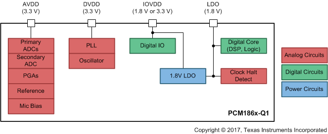 Figure 68. PCM186x-Q1 Power Distribution Tree
The PCM186x-Q1 uses a combination of 3.3-V functional blocks and 1.8-V functional blocks to achieve high analog performance, combined with high levels of digital integration. As such, the device has three internal power rails. AVDD provides the analog circuits with a clean 3.3-V rail. DVDD is used for 3.3-V digital clock circuits. Externally, AVDD and DVDD can be connected together without significant impact to performance. The final rail, IOVDD, is used for driving the input/output digital circuitry.
The PCM186x-Q1 integrates an on-chip LDO to convert an external 3.3 V to the 1.8 V required by the digital core. The LDO input is derived from IOVDD. Power-supply pin descriptions are listed in Table 24.
Table 24. Power-Supply Pin Descriptions
| NAME | DESCRIPTION |
|---|---|
| AVDD | Analog voltage supply (3.3 V) that powers the ADC, PGA, reference, and secondary ADC. |
| DVDD | Digital voltage supply (3.3 V) that is used for the PLL and the oscillator circuit. |
| IOVDD | Input/output pin voltage. Also used as a source for the internal LDO for the digital circuit. |
| LDO | Output from the on-chip LDO that is used with a 0.1-µF decoupling capacitor. Can be driven (used as power input) with a 1.8-V supply to bypass the on-chip LDO for lower power consumption. |
| AGND | Analog ground |
| DGND | Digital ground |
11.2 1.8-V Support
All PCM186x-Q1 devices can support external devices with a 1.8 V I/O. This operating mode is configured by driving IOVDD and LDO with 1.8 V.
11.3 Brownout Conditions
The PCM186x-Q1 devices do not have a brownout detector, or a reset pin to hold while the system is powering up. Make sure that the system design meets minimum AVDD, DVDD and IOVDD requirements.
11.4 Power-Up Sequence
The power-up sequence consists of the following steps:
11.5 Lowest Power-Down Modes
To achieve the lowest levels of power down and sleep current, the following recommended write sequences are suggested on PCM186x-Q1 software-controlled devices:
11.5.1 Lowest Power In Standby Mode (AVDD = DVDD = IOVDD = 3.3 V)
Consumption as low as 0.59 mW
0x00=0x00 //select page0
0x70=0x14 //power down reference
0x00=0x03 //select page3
0x12=0x41 //disable OSC
0x00=0x00 //select page0
11.5.2 Lowest Power in Sleep or Energysense Mode (AVDD = DVDD = IOVDD = 3.3 V)
Consumption as low as 14 mW
Clocks must be running during this process
0x00=0x00 //select page0
0x70=0x72 //enter in sleep mode
0x00=0xfd //select page253
0x14=0x10 //change global bias current
0x00=0x00 //select page0
Now stop the clocks
11.5.3 Lower Power in Sleep or Energysense Mode (AVDD = DVDD 3.3 V and IOVDD = 1.8 V)
Consumption as low as 11.15 mW
Clocks must be running during this process
0x00=0x00 //select page0
0x70=0x72 //enter in sleep mode
0x00=0xfd //select page253
0x14=0x10 //change global bias current
0x00=0x00 //select page0
stop the clocks (note: make sure the clock IO is 1.8 V)
11.6 Power-On Reset Sequencing Timing Diagram
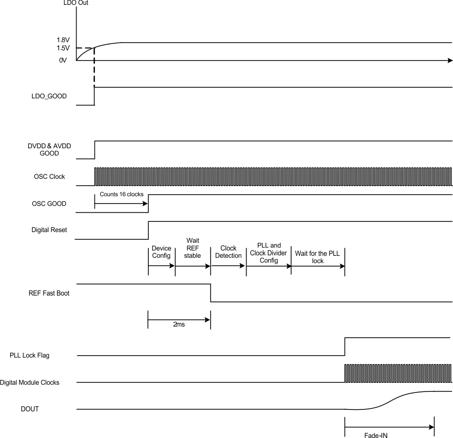 Figure 69. Power-On Reset Timing Diagram
11.7 Power Connection Examples
11.7.1 3.3-V AVDD, DVDD, and IOVDD Example
This example shows the most typical usage. One single supply, shared between all three supply voltage inputs. Rail-connected decoupling capacitors are not shown. Figure 70 shows 3.3-V supply for all supplies. Figure 71 shows separate 3.3 V for AVDD and DVDD.
NOTE
There is no disadvantage in separating the AVDD and DVDD, as the device waits until both are present before powering up.
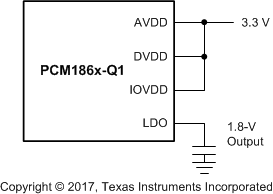 Figure 70. 3.3 V for All Supplies
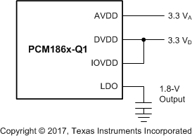 Figure 71. Separate 3.3 V for AVDD and DVDD
11.7.2 3.3-V AVDD, DVDD With 1.8-V IOVDD Example for Lower-Power Applications
The PCM186x-Q1 also supports interfacing to lower power 1.8-V processors, as shown in Figure 72. In the presence of an external 1.8 V connected to LDO, the internal LDO that takes DVDD (3.3 V) and converts it to the 1.8-V core voltage is bypassed. Under such conditions, IOVDD will then be used as the 1.8-V source for the digital core of the device. In such systems, it is still important to have 3.3 V for DVDD, as specific sections of the digital core in the device run from 3.3 V.
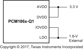 Figure 72. 1.8-V IOVDD With 3.3 V for AVDD and DVDD
11.8 Fade In
This sequence is the final stage of the power up and is illustrated in Figure 73. After the PLL has locked, the ADC starts running, and the data follows the fade-in sequence according to the following steps:
- Detect a zero crossing audio input.
- Increment the volume towards 0 dB with S-shaped volume.
- Repeat from step 1 until the result is 0 dB. The number of steps from mute to 0 dB is 48 steps.
- If zero crossing does not occur for 8192 sample times (= time out), change the volume-per-sample time.
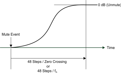 Figure 73. S-Curve Fade-In Behavior