SLASE64A December 2014 – June 2017 PCM1860-Q1 , PCM1861-Q1 , PCM1862-Q1 , PCM1863-Q1 , PCM1864-Q1 , PCM1865-Q1
PRODUCTION DATA.
- 1 Features
- 2 Applications
- 3 Description
- 4 Revision History
- 5 Device Comparison Table
- 6 Pin Configuration and Functions
-
7 Specifications
- 7.1 Absolute Maximum Ratings
- 7.2 ESD Ratings
- 7.3 Recommended Operating Conditions
- 7.4 Thermal Information
- 7.5 Electrical Characteristics: PGA and ADC AC Performance
- 7.6 Electrical Characteristics: DC
- 7.7 Electrical Characteristics: Digital Filter
- 7.8 Timing Requirements: External Clock
- 7.9 Timing Requirements: I2C Control Interface
- 7.10 Timing Requirements: SPI Control Interface
- 7.11 Timing Requirements: Audio Data Interface for Slave Mode
- 7.12 Timing Requirements: Audio Data Interface for Master Mode
- 7.13 Typical Characteristics
- 8 Parameter Measurement Information
-
9 Detailed Description
- 9.1 Overview
- 9.2 Functional Block Diagrams
- 9.3
Features Description
- 9.3.1 Analog Front End
- 9.3.2 Microphone Support
- 9.3.3 Input Multiplexer (PCM1860-Q1 and PCM1861-Q1)
- 9.3.4 Mixers and Multiplexers (PCM1862-Q1, PCM1863-Q1, PCM1864-Q1, and PCM1865-Q1)
- 9.3.5 Programmable Gain Amplifier
- 9.3.6 Automatic Clipping Suppression
- 9.3.7 Zero Crossing Detect
- 9.3.8 Digital Inputs
- 9.3.9
Clocks
- 9.3.9.1 Description
- 9.3.9.2 External Clock-Source Limits
- 9.3.9.3 Device Clock Distribution and Generation
- 9.3.9.4
Clocking Modes
- 9.3.9.4.1 Clock Configuration and Selection for Hardware-Controlled Devices
- 9.3.9.4.2 Clock Sources for Software-Controlled Devices
- 9.3.9.4.3 Clocking Configuration and Selection for Software-Controlled Devices
- 9.3.9.4.4 BCK Input Slave PLL Mode
- 9.3.9.4.5 Software-Controlled Devices ADC Non-Audio MCK PLL Mode
- 9.3.9.5 Software-Controlled Devices Manual PLL Calculation
- 9.3.9.6 Clock Halt and Error
- 9.3.9.7 Clock Halt and Error Detect
- 9.3.9.8 Changes in Clock Sources and Sample Rates
- 9.3.10 Analog-to-Digital Converters (ADCs)
- 9.3.11 Energysense
- 9.3.12 Audio Processing
- 9.3.13 Fade-In and Fade-Out Functions
- 9.3.14 Mappable GPIO Pins
- 9.3.15 Interrupt Controller
- 9.3.16 Audio Format Selection and Timing Details
- 9.4 Device Functional Modes
- 9.5 Programming
-
10Application and Implementation
- 10.1 Application Information
- 10.2 Typical Applications
- 11Power Supply Recommendations
- 12Layout
-
13Register Map
- 13.1 Register Map Description
- 13.2 Register Map Summary
- 13.3
Page 0 Registers
- 13.3.1 Page 0: Register 1 (address = 0x01) [reset = 0x00]
- 13.3.2 Page 0: Register 2 (address = 0x02) [reset = 0x00]
- 13.3.3 Page 0: Register 3 (address = 0x03) [reset = 0x00]
- 13.3.4 Page 0: Register 4 (address = 0x04) [reset = 0x00]
- 13.3.5 Page 0: Register 5 (address = 0x05) [reset = 0x86]
- 13.3.6 Page 0: Register 6 (address = 0x06) [reset = 0x41]
- 13.3.7 Page 0: Register 7 (address = 0x07) [reset = 0x41]
- 13.3.8 Page 0: Register 8 (address = 0x08) [reset = 0x42]
- 13.3.9 Page 0: Register 9 (address = 0x09) [reset = 0x42]
- 13.3.10 Page 0: Register 10 (address = 0x0A) [reset = 0x00]
- 13.3.11 Page 0: Register 11 (address = 0x0B) [reset = 0x44]
- 13.3.12 Page 0: Register 12 (address = 0x0C) [reset = 0x00]
- 13.3.13 Page 0: Register 13 (address = 0x0D) [reset = 0x00]
- 13.3.14 Page 0: Register 14 (address = 0x0E) [reset = 0x00]
- 13.3.15 Page 0: Register 15 (address = 0x0F) [reset = 0x00]
- 13.3.16 Page 0: Register 16 (address = 0x10) [reset = 0x01]
- 13.3.17 Page 0: Register 17 (address = 0x11) [reset = 0x20]
- 13.3.18 Page 0: Register 18 (address = 0x12) [reset = 0x00]
- 13.3.19 Page 0: Register 19 (address = 0x13) [reset = 0x00]
- 13.3.20 Page 0: Register 20 (address = 0x14) [reset = 0x00]
- 13.3.21 Page 0: Register 21 (address = 0x15) [reset = 0x00]
- 13.3.22 Page 0: Register 22 (address = 0x16) [reset = 0x00]
- 13.3.23 Page 0: Register 23 (address = 0x17) [reset = 0x00]
- 13.3.24 Page 0: Register 24 (address = 0x18) [reset = 0x00]
- 13.3.25 Page 0: Register 25 (address = 0x19) [reset = 0x00]
- 13.3.26 Page 0: Register 26 (address = 0x1A) [reset = 0x00]
- 13.3.27 Page 0: Register 27 (address = 0x1B) [reset = 0x00]
- 13.3.28 Page 0: Register 32 (address = 0x20) [reset = 0x01]
- 13.3.29 Page 0: Register 33 (address = 0x21) [reset = 0x00]
- 13.3.30 Page 0: Register 34 (address = 0x22) [reset = 0x01]
- 13.3.31 Page 0: Register 35 (address = 0x23) [reset = 0x03]
- 13.3.32 Page 0: Register 37 (address = 0x25) [reset = 0x07]
- 13.3.33 Page 0: Register 38 (address = 0x26) [reset = 0x03]
- 13.3.34 Page 0: Register 39 (address = 0x27) [reset = 0x3F]
- 13.3.35 Page 0: Register 40 (address = 0x28) [reset = 0x01]
- 13.3.36 Page 0: Register 41 (address = 0x29) [reset = 0x00]
- 13.3.37 Page 0: Register 42 (address = 0x2A) [reset = 0x00]
- 13.3.38 Page 0: Register 43 (address = 0x2B) [reset = 0x01]
- 13.3.39 Page 0: Register 44 (address = 0x2C) [reset = 0x00]
- 13.3.40 Page 0: Register 45 (address = 0x2D) [reset = 0x00]
- 13.3.41 Page 0: Register 48 (address = 0x30) [reset = 0x00]
- 13.3.42 Page 0: Register 49 (address = 0x31) [reset = 0x00]
- 13.3.43 Page 0: Register 50 (address = 0x32) [reset = 0x00]
- 13.3.44 Page 0: Register 51 (address = 0x33) [reset = 0x00]
- 13.3.45 Page 0: Register 52 (address = 0x34) [reset = 0x00]
- 13.3.46 Page 0: Register 54 (address = 0x36) [reset = 0x01]
- 13.3.47 Page 0: Register 64 (address = 0x40) [reset =0x80]
- 13.3.48 Page 0: Register 65 (address = 0x41) [reset = 0x7F]
- 13.3.49 Page 0: Register 66 (address = 0x42) [reset = 0x00]
- 13.3.50 Page 0: Register 67 (address = 0x43) [reset = 0x80]
- 13.3.51 Page 0: Register 68 (address = 0x44) [reset = 0x7F]
- 13.3.52 Page 0: Register 69 (address = 0x45) [reset = 0x00]
- 13.3.53 Page 0: Register 70 (address = 0x46) [reset = 0x80]
- 13.3.54 Page 0: Register 71 (address = 0x47) [reset = 0x7F]
- 13.3.55 Page 0: Register 72 (address = 0x48) [reset = 0x00]
- 13.3.56 Page 0: Register 73 (address = 0x49) [reset = 0x80]
- 13.3.57 Page 0: Register 74 (address = 0x4A) [reset = 0x7F]
- 13.3.58 Page 0: Register 75 (address = 0x4B) [reset = 0x00]
- 13.3.59 Page 0: Register 76 (address = 0x4C) [reset = 0x80]
- 13.3.60 Page 0: Register 77 (address = 0x4D) [reset = 0x7F]
- 13.3.61 Page 0: Register 78 (address = 0x4E) [reset = 0x00]
- 13.3.62 Page 0: Register 79 (address = 0x4F) [reset = 0x80]
- 13.3.63 Page 0: Register 80 (address = 0x50) [reset = 0x7F]
- 13.3.64 Page 0: Register 81 (address = 0x51) [reset = 0x00]
- 13.3.65 Page 0: Register 82 (address = 0x52) [reset = 0x80]
- 13.3.66 Page 0: Register 83 (address = 0x53) [reset = 0x7F]
- 13.3.67 Page 0: Register 84 (address = 0x54) [reset = 0x00]
- 13.3.68 Page 0: Register 85 (address = 0x55) [reset = 0x80]
- 13.3.69 Page 0: Register 86 (address = 0x56) [reset = 0x7F]
- 13.3.70 Page 0: Register 87 (address = 0x57) [reset = 0x00]
- 13.3.71 Page 0: Register 88 (address = 0x58) [reset = 0x00]
- 13.3.72 Page 0: Register 89 (address = 0x59) [reset = 0x00]
- 13.3.73 Page 0: Register 90 (address = 0x5A) [reset = 0x00]
- 13.3.74 Page 0: Register 96 (address = 0x60) [reset = 0x01]
- 13.3.75 Page 0: Register 97 (address = 0x61) [reset = 0x00]
- 13.3.76 Page 0: Register 98 (address = 0x62) [reset =0x10]
- 13.3.77 Page 0: Register 112 (address = 0x70) [reset = 0x70]
- 13.3.78 Page 0: Register 113 (address = 0x71) [reset = 0x10]
- 13.3.79 Page 0: Register 114 (address = 0x72) [reset = 0x00]
- 13.3.80 Page 0: Register 115 (address = 0x73) [reset = 0x00]
- 13.3.81 Page 0: Register 116 (address = 0x74) [reset = 0x00]
- 13.3.82 Page 0: Register 117 (address = 0x75) [reset = 0x00]
- 13.3.83 Page 0: Register 120 (address = 0x78) [reset = 0x00]
- 13.4
Page 1 Registers
- 13.4.1 Page 1: Register 1 (address = 0x01) [reset = 0x00]
- 13.4.2 Page 1: Register 2 (address = 0x02) [reset = 0x00]
- 13.4.3 Page 1: Register 4 (address = 0x04) [reset = 0x00]
- 13.4.4 Page 1: Register 5 (address = 0x05) [reset = 0x00]
- 13.4.5 Page 1: Register 6 (address = 0x06) [reset = 0x00]
- 13.4.6 Page 1: Register 7 (address = 0x07) [reset = 0x00]
- 13.4.7 Page 1: Register 8 (address = 0x08) [reset = 0x00]
- 13.4.8 Page 1: Register 9 (address = 0x09) [reset = 0x00]
- 13.4.9 Page 1: Register 10 (address = 0x0A) [reset = 0x00]
- 13.4.10 Page 1: Register 11 (address = 0x0B) [reset = 0x00]
- 13.5 Page 3 Registers
- 13.6 Page 253 Registers
- 14Device and Documentation Support
- 15Mechanical, Packaging, and Orderable Information
Package Options
Mechanical Data (Package|Pins)
- DBT|30
Thermal pad, mechanical data (Package|Pins)
Orderable Information
9 Detailed Description
9.1 Overview
The PCM186x-Q1 family of automotive-audio, analog-to-digital converters (ADCs) features a highly flexible, audio front end that supports input levels from small millivolt microphone inputs to 2.1-VRMS line inputs. The analog front end can be configured to support either differential or single-ended inputs, providing optimal performance when using differential inputs. Mixing single-ended and differential inputs is possible. A digital microphone interface is available in the software-controlled devices.
These devices support advanced clocking with the aid of an integrated oscillator circuit and an on-chip analog phase-locked loop (PLL). The integrated oscillator circuit allows for the use of an external crystal or an external master clock as the clock source in master mode. In addition, the PLL can be used to generate an on-chip master clock that can be shared with the rest of the system, all from a bit clock input. This feature is useful in systems where the audio source has no master clock to drive digital-to-analog converters (DACs) and amplifiers. The on-chip clock monitoring system can also be monitored by the system microcontroller, in case clocks are lost and the device enters sleep or standby state.
The secondary analog-to-digital converter (ADC) is a low-power, non-audio ADC that is used in sleep mode to monitor the analog inputs. The secondary ADC is also used in controlsense mode to measure dc voltages in a system, such as battery voltage and control potentiometers. In addition, controlsense features offer an option to generate interrupts after detected voltages cross specific thresholds, allowing the microcontroller to be in a lower-power sleep mode while the control voltages being measured are stable.
Control registers in this data sheet are shown as REGISTER_BIT_or_BYTE_NAME (page.x hex_address).
9.2 Functional Block Diagrams
The high level block diagrams, Figure 23 to Figure 25, show the differences between the PCM186x-Q1 family. An internal block diagram of the PCM186x-Q1 family is shown in Figure 26.
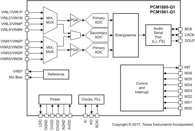 Figure 23. PCM1860-Q1 and PCM1861-Q1
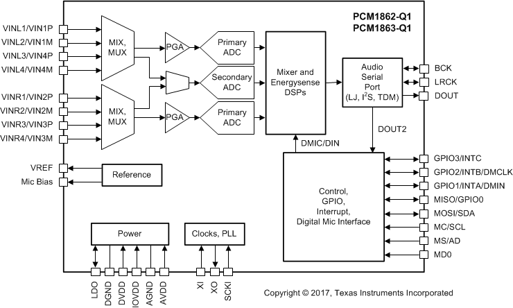 Figure 24. PCM1862-Q1 and PCM1863-Q1
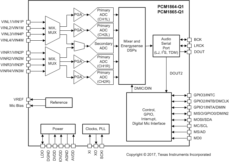 Figure 25. PCM1864-Q1 and PCM1865-Q1
Power supplies and references have been omitted from this diagram for simplicity. Dotted lines, for the programmable gain amplifier (PGA) and the additional ADCs, are for the 4-channel devices only. Greyed-out pins are multifunction pins only.
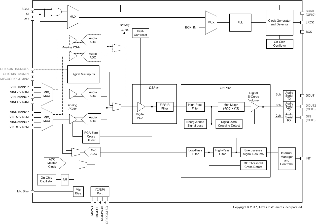 Figure 26. Internal Block Diagram of the PCM186x-Q1
9.3 Features Description
9.3.1 Analog Front End
The PCM186x-Q1 has a flexible front end that accepts either differential or single-ended inputs. The device supports up to 2.1 VRMS in single-ended mode, and up to 4.2 VRMS in differential mode.
The MIX and MUX circuit before the PGA allows the analog inputs to be mixed and multiplexed in both single-ended and differential modes. Mixing functionality is available in software-controlled devices only. No individual gain controls are available before the PGA. A high-level diagram of the front-end circuitry is shown in Figure 27.
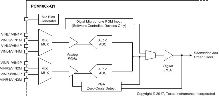 Figure 27. High Level View of PCM186x-Q1 Front End-Circuitry
DC blocking capacitors are required on the analog inputs to make sure that correct dc bias conditions are established. Because the value of the output short-circuit protection resistor in the source product is typically unknown, issues such as gain error and dc shift may occur if dc blocking capacitors are not used.
For systems where external amplifiers are used before the PCM186x-Q1, dc blocking capacitors are still recommended because the input pins are designed to bias to AVDD / 2. The common mode voltage range is still limited to the maximum input voltage of the device.
Do not connect unused analog input pins.
9.3.2 Microphone Support
The PCM186x-Q1 supports analog and digital microphones. Analog signals are treated the same way as line-level signals, except for the requirement for mic bias. Digital microphone Inputs (PDM inputs) use GPIOs on the device. Two-channel ADC variants of the PCM186x-Q1 family can support two digital microphones using a single data pin and a single clock pin. The 4-channel variants can support up to 4 digital microphones (2 data pins).
The PCM1860-Q1 and PCM1861-Q1 offer three pin-selectable gain options, 0 dB, 12 dB, or 32 dB.
The PCM1862-Q1, PCM1863-Q1, PCM1864-Q1, and PCM1865-Q1 offer programmable gain options from –12 dB to +32 dB with –0.5-dB step intervals.
Digital microphones typically have a PDM output that can be brought into an ADC digital decimation filter. PDM microphones require power and a clock. Power should be handled from an external source.
Digital microphone mode gain can be added in the digital PGA and in the mixer. In digital microphone mode, the PCM1862-Q1 and PCM1863-Q1 offer up to 18-dB gain (mixer only); whereas, the PCM1864-Q1 and PCM1865-Q1 offer up to 30-dB gain (18 dB from mixer and 12 dB from digital PGA).
On the PCM1864-Q1 and PCM1865-Q1, a 2-channel digital mic + 2-channel ADC mode is possible. With the PCM1862-Q1 or PCM1863-Q1, four channels are only possible with a ADC + I2S input configuration.
9.3.2.1 Mic Bias
The PCM186x-Q1 can provide a microphone bias to power and bias microphones at 2.6 V on pin 5. Decouple or filter the Mic Bias pin with an external capacitor. Mic Bias is typically used with a electret microphone. The internal regulator, as well as an on-chip terminating resistor to GND can also be enabled using register MIC_BIAS_CTRL (Page.3, 0x15). By default, the device is configured to bypass the on-chip resistor. The mic bias pin can be left unconnected if not used.
9.3.3 Input Multiplexer (PCM1860-Q1 and PCM1861-Q1)
The hardware-controlled devices can support a wide gain range using the MD2, MD5 and MD6 configuration pins as shown in Table 1.
Table 1. Channel and Gain Selection for Hardware-Controlled Devices
| MD6 | MD5 | MD2 | ADC1_L / PGA1_L | ADC1_R / PGA1_R |
|---|---|---|---|---|
| L | L | L | S.E - VINL1 / 0 dB | S.E - VINR1 / 0 dB |
| L | L | H | S.E - VINL2 / 0 dB | S.E - VINR2 / 0 dB |
| L | H | L | S.E - VINL3 / 0 dB | S.E - VINR3 / 0 dB |
| L | H | H | S.E - VINL4 / 0 dB | S.E - VINR4 / 0 dB |
| H | L | L | S.E - VINL4 / 12 dB | S.E - VINR4 / 12 dB |
| H | L | H | S.E - VINL4 / 32 dB | S.E - VINR4 / 32 dB |
| H | H | L | Diff(VIN1P/VIN1M) / 0 dB | Diff(VIN2P/VIN2M) / 0 dB |
| H | H | H | Diff(VIN3P/VIN3M) / 12 dB | Diff(VIN4P/VIN4M) / 12 dB |
9.3.4 Mixers and Multiplexers (PCM1862-Q1, PCM1863-Q1, PCM1864-Q1, and PCM1865-Q1)
The PCM186x-Q1 software-controlled devices offer a mix and multiplex level of functionality on the front end, as shown in Figure 27. The switches integrated into the multiplexer can also be switched on in parallel, offering a direct mix of inputs. This function can be selected by register for each ADC input selection, ADCX1_INPUT_SEL_X (Page.0, 0x06 → 0x09). In single ended mode, each Audio ADC is tightly coupled to a dedicated PGA and MUX. ADC1L (and ADC2L on the PCM1864-Q1 and PCM1865-Q1) is connected a mux that has input pins VINLx, (x = 1 to 4). ADC1R (and ADC2R on the PCM1864-Q1 and PCM1865-Q1) is connected to a mux that has input pins VINRx (x = 1 to 4).
Mixing between the left channels of stereo pairs is possible in the mux dedicated to ADC1L and right channels of stereo pairs in the mux dedicated to ADC1R. In addition, polarity of the inputs can be inverted using the MSB of the select register. Mixing left and right sources to create mono mixes can only be done in the digital mixer, post ADC conversion, or alternatively, other analog inputs can be connected for mixing.
The examples available are shown in Table 2, where [SE] is single-ended, and [DIFF] is a differential input.
Table 2. MUX, MIX, and Polarity Input Selection(1)
| REGISTER CODE | ADC1L AND ADC2L | ADC1R AND ADC2R |
|---|---|---|
| 0x00 | No Selection (Mute) | No Selection (Mute) |
| 0x01 | VINL1[SE] (Default) | VINR1[SE] (Default) |
| 0x02 | VINL2[SE] | VINR2[SE] |
| 0x03 | VINL2[SE] + VINL1[SE] | VINR2[SE] + VINR1[SE] |
| 0x04 | VINL3[SE] | VINR3[SE] |
| 0x05 | VINL3[SE] + VINL1[SE] | VINR3[SE] + VINR1[SE] |
| 0x06 | VINL3[SE] + VINL2[SE] | VINR3[SE] + VINR2[SE] |
| 0x07 | VINL3[SE] + VINL2[SE] + VINL1[SE] | VINR3[SE] + VINR2[SE] + VINR1[SE] |
| 0x08 | VINL4[SE] | VINR4[SE] |
| 0x09 | VINL4[SE] + VINL1[SE] | VINR4[SE] + VINR1[SE] |
| 0x0A | VINL4[SE] + VINL2[SE] | VINR4[SE] + VINR2[SE] |
| 0x0B | VINL4[SE] + VINL2[SE] + VINL1[SE] | VINR4[SE] + VINR2[SE] + VINR1[SE] |
| 0x0C | VINL4[SE] + VINL3[SE] | VINR4[SE] + VINR3[SE] |
| 0x0D | VINL4[SE] + VINL3[SE] + VINL1[SE] | VINR4[SE] + VINR3[SE] + VINR1[SE] |
| 0x0E | VINL4[SE] + VINL3[SE] + VINL2[SE] | VINR4[SE] + VINR3[SE] + VINR2[SE] |
| 0x0F | VINL4[SE] + VINL3[SE] + VINL2[SE] + VINL1[SE] | VINR4[SE] + VINR3[SE] + VINR2[SE] + VINR1[SE] |
| 0x10 | {VIN1P, VIN1M}[DIFF] | {VIN2P, VIN2M}[DIFF] |
| 0x20 | {VIN4P, VIN4M}[DIFF] | {VIN3P, VIN3M}[DIFF] |
| 0x30 | {VIN1P, VIN1M}[DIFF] + {VIN4P, VIN4M}[DIFF] | {VIN2P, VIN2M}[DIFF] + {VIN3P, VIN3M}[DIFF] |
9.3.5 Programmable Gain Amplifier
The PCM186x-Q1 has a two-stage programmable gain amplifier (PGA). Coarse gain adjustment is done in the analog domain, and fine gain adjustment is done in the digital domain. The ±12-dB analog gain steps are designed for varying line level inputs, whereas the 20 dB and 32 dB are primarily designed for microphone inputs, and will likely need additional gain that can be done in the digital domain. The analog gain steps between –12 dB and +12 dB are in 1-dB steps. Half-dB steps between those points are done in the digital PGA. Gain steps between 12 dB and 20 dB are all done in the digital domain. (for example, 18-dB gain = 12-dB analog + 6-dB digital). The gain structure in the PCM186x-Q1 is shown in Figure 28.
 Figure 28. PCM186x-Q1 Complete Gain Structure (PGAs and Attenuator)
The analog gain steps within the analog PGA are shown in Figure 29. Again, from –12 dB to +12 dB, the steps are 1 dB each. The digital PGA has granularity down to 0.5 dB.
 Figure 29. Analog Gain Steps With Software-Controlled Devices
The PGA in the PCM186x-Q1 is a hybrid analog and digital programmable gain amplifier. The devices integrate a lookup table with the optimal gain balance between analog and digital gain, allowing the gain to be set in a single register per channel. For example, set 18 dB gain, and the system allocates 12 dB to the analog PGA, and 6 dB to the digital PGA. This function is called auto gain mapping.
The PGA is a zero crossing detect type, and has the ability to set target gain, and have the device work towards it (with a timeout if there is no zero crossing). Any changes in the Analog PGA and digital PGA are designed to step towards the final level. However, any changes in the mixer PGA are immediate. Take care when changing gain levels in the digital mixer PGA. Alternatively, multiple writes can be made of small enough values that do not cause significant pops or clicks.
NOTE
Changing gain in the PGA requires the on-chip DSP to be clocked. The DSP is used to calculate the steps to the target gain. This is not an issue in master mode, but can be a challenge in slave mode, if the system master is not active yet.
For example, if the current level = 0 dB, then set the target as 3.5 dB. The PGA then increases gain in 0.5-dB steps towards 3.5 dB.
The auto gain mapping function can by bypassed if required, using manual gain mapping. Manual gain mapping is useful when using digital microphones, as the PDM input signal bypasses the analog PGA and must be amplified using the digital PGA. (PGA_MODE (Page.0, 0x19). Digital PGA update is only available in the 4-channel devices because the digital gain in 2-channel devices is fixed to 0 dB when manual gain mapping is enabled.
NOTE
Using the device with a differential inputs increases the full-scale voltage to 4.2 VRMS (that's 2.1 VRMS per pin, out of phase).
9.3.6 Automatic Clipping Suppression
The PCM186x-Q1 software-controlled devices have the ability to automatically lower the gain in 0.5 dB steps under the following conditions if the ADC is clipping.
The device detects clipping after the decimation filter in the signal chain, shown in Figure 30, and counts the number of successive clips before responding.
The device also generates an internal interrupt that can be mapped to a GPIO or interrupt pin, allowing the system microcontroller to make the decision to increase the gain and consider the clipping an isolated event, or make the decision that the new gain setting is appropriate.
 Figure 30. Sampling Points Within the PCM186x-Q1 for Auto Clipping Suppression
9.3.6.1 Attenuation Level
This feature is not designed to be a complete analog gain control. This feature was defined to avoid clipping, and to inform the system microcontroller of a clipping event, to allow the microcontroller (or the end user) to decide if the gain should be increased again.
The attenuation is programmable to –3 dB, –4 dB, –5 dB, or –6 dB.
9.3.6.2 Channel Linking
Depending on the application, users may not want to link input channels, however, for the majority of stereo input applications, its strongly recommended to set the system to track gain across inputs, to maintain balance.
The auto PGA clipping suppression control has the settings shown in Table 3.
Table 3. Auto Clipping Suppression Control Registers
| REGISTER NAME | REGISTER LOCATION | USAGE | VALUES |
|---|---|---|---|
| AGC_EN | Pg0 0x05 | Enable auto gain control | 0: Disable (Default) 1: Enable |
| CLIP_NUM[1:0] | Pg0 0x05 | Start auto gain control after detects CLIP_NUM times of ADC sample clips | 0: 80 1: 40 2: 20 3: 10 (Default) |
| MAX_ATT[1:0] | Pg0 0x05 | Maximum automatic attenuation | 0: –3 dB (Default) 1: –4 dB 2: –5 dB 3: –6 dB |
| DPGA_CLIP_EN | Pg0 0x05 | Enable clipping detection after the digital PGA. Note that digital PGA is post ADC, meaning that there is a short delay before clipping is detected. | 0: Disable (Default) 1: Enable |
| LINK | Pg0 0x05 | Link all channels together if dealing with stereo sources to maintain balance. | 0: Independent control (Default) 1: Ch1[R]/Ch2[L]/Ch2[R] follow Ch1[L] PGA value. |
| SMOOTH | Pg0 0x05 | Enable smooth transition from step to step (zero crossing). | 0: Immediate change 1: Smooth change (default) |
9.3.7 Zero Crossing Detect
The PCM186x-Q1 uses a zero crossing detector to make gain changes only when the incoming signal crosses the halfway point between negative and positive swing, reducing zipper noise.
There are two sources for the controller, the output of the ADC modulator and the output from the digital PGA. The analog PGA is sampled at four times the audio sampling rate to detect the zero crossing. The digital PGA is sampled at a similar rate.
The process for changing gain in the PCM186x-Q1 is as follows:
- Detect a zero crossing of the oversampled analog input channel.
- Increment or decrement the gain toward the target PGA value step by 0.5 dB.
- Repeat from (1) until arrival at the target PGA value.
- If zero crossing does not occur for 8192 sample times (= time out), change the gain per sample.
This process does not require intervention by the user. This data serves as information only. Also, please note that DSPs must be running (clocked) for this functionality to work.
9.3.8 Digital Inputs
9.3.8.1 Stereo PCM Sources
The PCM186x-Q1 can support stereo PCM data on GPIO pins so that I2S sources, such as wireless modules can have their data mixed with the incoming analog content. The clock rate of the incoming data (known as DIN) must be synchronous with the PCM186x-Q1 software-controlled device main clocks. There is no integrated sample rate converter on-chip. The DIN signal can be received on GPIO0, 1, 2, or 3, and configured on GPIO_FUNC_X (Page.0 0x10 and 0x11). The incoming data are then driven to the digital mixer running on DSP2.
The audio format can be configured separately from the output serial port using register RX_TDM_OFFSET (P0, 0x0E).
Inputs can be mixed and volume-controlled before routing to a digital amplifier. Typical uses could be the connection to a Bluetooth™ module. The mixing and crossfading is done all in the PCM186x-Q1, rather than a hard switch in external logic. The on-chip PLL also helps create the system master clock (SCKOUT) for poorly designed I2S Bluetooth modules that do not provide a system clock to drive the system DACs.
If the stereo PCM data source has a requirement to drive the audio clock pins when transmitting in a system where the PCM186x-Q1 has not been set to slave yet, the PCM186x-Q1 does not suffer any damage during clock driver contention. However, the PCM186x-Q1 will have some irregular output due to clock errors. In systems with additional stereo PCM sources that need to be master (such as a S/PDIF receive), set the PCM186x-Q1 to always be a clock slave, or switch the device from master to slave mode, before enabling the stereo PCM source.
9.3.8.2 Digital PDM Microphones
Up to four digital microphones are supported on the PCM1864-Q1 and PCM1865-Q1, using a shared output clock (configured from GPIO2) and two data lines, GPIO0 or GPIO1. Two digital microphones are supported on the PCM1862-Q1 and PCM1863-Q1, mainly using GPIO1 as the data input. The PCM1860-Q1 or PCM1861-Q1 does not support digital microphones. The typical connection and protocol diagrams for these microphones are shown in Figure 31 and Figure 32.
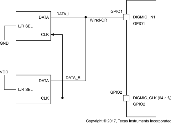 Figure 31. Digital Microphone Example Connection
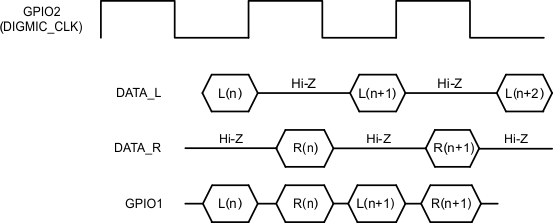 Figure 32. Digital Microphone Protocol
Supported Digital Microphone clock frequency is as follows, and the frequency depends on required operating sampling frequency as follows:
- 2.0480 MHz (32 kHz × 64)
- 2.8224 MHz (44.1 kHz × 64)
- 3.072 MHz (48 kHz × 64)
- 3.072 MHz (96 kHz × 32 )
- Sampling frequency is 32 kHz or 44.1 kHz
- SCK is 256 × fS.
- Enable Auto Clock Detector (Default)
9.3.9 Clocks
9.3.9.1 Description
The PCM186x-Q1 family has an extremely flexible clocking architecture. All converters require a master clock (typically, a 2n power of the sampling rate known as MCK), a bit clock (BCK) that is used to clock the data bit-by-bit out of the device (typically running at 64-fS to allow up to 32 bits per channel output), and finally a wordclock (left-right clock, LRCK) that is used to set the exact sampling point for the ADC.
The PCM186x-Q1 family can be a clock master (where BCK and LRCK can be internally divided from a provided master clock) or can be a clock slave, where all clocks (MCK, BCK and LRCK) must be provided by an external source.
Unlike many competing devices, the PCM186x-Q1 family can source its master clock from two different sources, either an external crystal, or a CMOS level (3.3 V or 1.8 V) clock, eliminating the usual external crystal oscillator circuit required to source a CMOS clock signal.
The PCM186x-Q1 also differentiates itself by integrating an on-chip phase locked loop (PLL) that can generate real audio-rate clocks from any clock source between 1 MHz and 50 MHz. The PCM1860-Q1 or PCM1861-Q1 hardware-controlled devices have the ability to detect an absence of MCK in slave mode and automatically generate a MCK signal. Software-controlled devices, such as the PCM1862-Q1, PCM1863-Q1, PCM1864-Q1 and PCM1865-Q1 can have their PLL programmed to generate audio clocks based on any incoming clock rate. For example, a 12 MHz clock in the system can be used to generate clocks for a 44.1-kHz system.
9.3.9.2 External Clock-Source Limits
The three different clock sources for the device each have some limits in terms of their input circuitry, as shown in Table 4. These limits are separate from the internal PLL capability.
On PCM1860-Q1 and PCM1861-Q1, the highest standard frequency supported by an XTAL is 96 kHz, because the lowest divider ratio of master clock to LRCK is 256 (24.576 MHz / 256 = 96 kHz). This limitation is not present in the software-controlled devices because the divider ratio is programmable. However, 192 kHz can be supported by using an external CMOS source.
Table 4. External Clock-Source Limitations and Notes
| CLOCK SOURCE | LIMITS | NOTES |
|---|---|---|
| XTAL | 15 MHz → 35 MHz | |
| 3.3-V CMOS MCLK | 1 MHz → 50 MHz | Should be input to SCKI pin. 3.3 V CMOS can be input, even when IOVDD is 1.8 V |
| 1.8-V CMOS MCLK | 1 MHz → 50 MHz | Should be input to XI pin. |
9.3.9.3 Device Clock Distribution and Generation
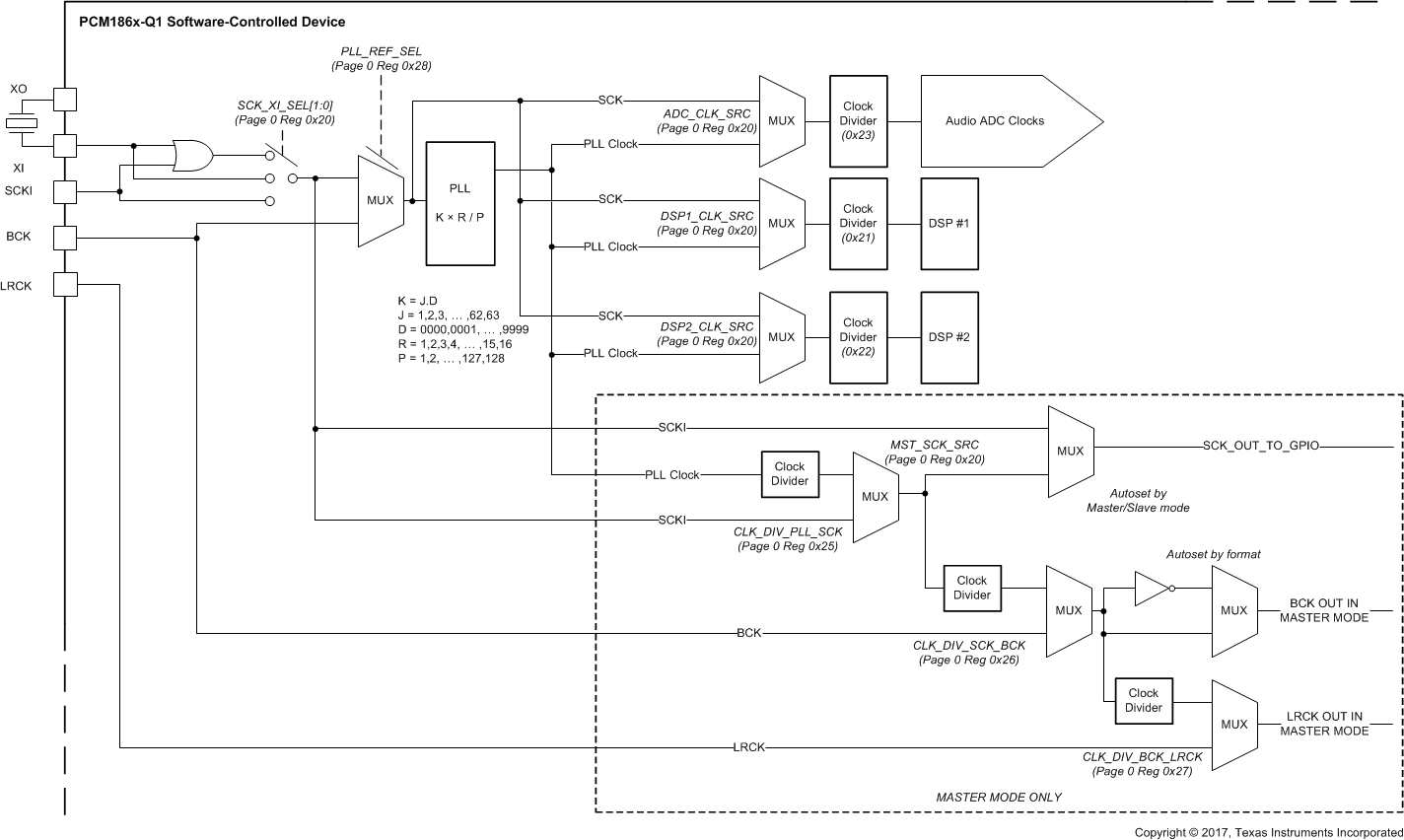
PLLs can be used in all modes to generate the clocks required to run both fixed-function DSPs. The dividers are automatically configured based on the clock rate detection. The clock architecture shown in Figure 33 allows non-audio clock sources to be used as clock sources and the PCM186x-Q1 to continue to run in a master mode, providing all PCM and I2S clocks for other converters in the system.
Target Clock Rates for the ADC, DSP1 and DSP2 can be seen in Table 9 and Table 10. In manual clock configuration modes, the dividers should be set to achieve these targets. In short, for 2-channel devices, DSP1 and DSP2 should be 256x the sampling rate; for 4-channel devices, DSP1 should be configured for 512x the sampling rate, and DSP2 should be 256x.
9.3.9.4 Clocking Modes
As shown in Table 5, there are four different clocking modes available on the device that take advantage of the onboard PLL and clock detection. Advanced clock detection and a smart internal state engine in the PCM186x-Q1 can automatically configure the various dividers in the device (see the Device Clock Distribution and Generation section) with optimized values. Automatic clock configuration is enabled by default, using the register CLKDET_EN (Page.0, 0x20).
Table 5. PCM186x-Q1 Clocking Modes
| NAME | DEVICE | External XTAL/MCK INPUT | BCK, LRCK DIRECTION | PLL CONFIGURATION |
|---|---|---|---|---|
| ADC master mode | PCM186x-Q1 | YES | OUT | Not required |
| ADC slave mode | PCM186x-Q1 | YES | IN | Not required |
| ADC slave PLL mode | PCM186x-Q1 | NO | IN | Automatic for standard audio rates |
| ADC non-audio MCK | PCM1862-Q1 PCM1863-Q1 PCM1864-Q1 PCM1865-Q1 |
YES | OUT | Manual |
9.3.9.4.1 Clock Configuration and Selection for Hardware-Controlled Devices
The PCM1860-Q1 and PCM1861-Q1 hardware-controlled devices offer both master and slave functionality. In master mode, a source master clock (of 256x, 384x, or 512x the sampling rate) can be sourced from either an external crystal (XI/XO) or on an incoming SCK. (see the External Clock-Source Limits section for input rate limitations on SCK sources) The clock from XI and SCK are OR-ed internally, allowing either to be used.
These hardware-controlled devices can generate the other I2S clocks (BCK and LRCK) in master mode (with dividers set in MD0 and MD1) or be a clock slave to MCK,BCK and LRCK. In this scenario, the device auto-detects the clock divider ratio.
In master mode, BCK per LRCK is fixed at 64, and allows up to 32 bits per channel.
Selection of the appropriate master or slave, and clock ratio between MCK and fS can be done using MD0 and MD1.
Table 6 shows the suggested master clock rates for each of the sample rates supported. For slave mode, set BCK per LRCK to 64.
Table 6. External Master Clock Rate Versus Sampling Frequency
| SAMPLING RATE FREQUENCY (kHz) |
SYSTEM CLOCK FREQUENCY (MHz) | ||||
|---|---|---|---|---|---|
| 256 × fS | 384 × fS | 512 × fS | |||
| 8.0 | 2.048 | 3.072 | 4.096 | ||
| 16.0 | 4.096 | 6.144 | 8.192 | ||
| 32.0 | 8.1920 | 12.2880 | 16.3840 | ||
| 44.1 | 11.2896 | 16.9344 | 22.5792 | ||
| 48.0 | 12.2880 | 18.4320 | 24.5760 | ||
| 64.0 | 16.3840 | 24.5760 | 32.7680 | ||
| 88.2 | 22.5792 | 33.8688 | 45.1584 | ||
| 96.0 | 24.5760 | 36.8640 | 49.1520 | ||
| 176.4 | 45.1584 | — | — | ||
| 192.0 | 49.1520 | — | — | ||
9.3.9.4.2 Clock Sources for Software-Controlled Devices
The PCM1862-Q1, PCM1863-Q1, PCM1864-Q1, and PCM1865-Q1 software-controlled devices support a wide range of options for generating the clocks required to operate the ADC section, as well as an interface and other control blocks, as shown in Figure 34.
The clocks for the PLL require a source reference clock. This clock source can be configured on software devices as the XTAL, SCK or BCK.
These software-controlled devices share a similar clock tree for the generation and distribution of clocks, as shown in Figure 33.
Register CLK_MODE (Page.0 0x20) is used to configure the clock configuration. Bits [5:7] configure the OR and MUX for the incoming MCLK.
Register MST_MODE (Page.0 0x20) is used to set the device in master or slave mode. Bits [1:3] set clock sources for the ADC, DSP1 and DSP2. These can mostly be ignored for the most common applications, but are provided for advanced users.
Register MST_SCK_SRC (Page.0 0x20) is used to set the source of the SCKO in master mode. The master mode BCK and LRCK will be a division of this. The selection is either SCKI/XTI or PLL. PLL can be used when you have a non-audio rate reference clock (BCK or SCKI), as well as when you have an SCKI that is much too slow for what is required for SCKO.
Most applications will use XTI/SCKI as the source for master mode SCK.
The CLKDET_EN (Page.0, 0x20) register bit (auto clock detector) is important; the clock detector is mainly functional for slave modes, and for master modes where the master clock is a 256×, 384×, or 512× multiple of the incoming data rate.
The relation between the master mode configuration registers is shown in Table 7.
NOTE
Non audio related master clock sources can be used with the PCM186x-Q1 software -controlled devices providing the PLL is programmed manually. CLKDET_EN should be set to 0.
The result of configurations can be checked by reading registers FS_INFO / CURRENT_BCK_RATIO (Page.0 0x73 and 0x74).
NOTE
In master mode on software-controlled devices, only the following BCK to LRCK ratios are supported: 32x, 48x, 64x and 256x. 128x is not supported
Table 7. Master Mode Clock Configuration Registers
9.3.9.4.3 Clocking Configuration and Selection for Software-Controlled Devices
9.3.9.4.3.1 Target Clock Rates for ADC, DSP1 and DSP2
The ADC, DSP1 and DSP2 each have specific minimum clock requirements that can be driven from either the incoming SCK or the output of the PLL, as shown in Table 8.
Table 8. Minimum Required Clock Ratios for ADC, DSP1 and DSP2
| CORE | 2-CHANNEL DEVICE RATIO | 4-CHANNEL DEVICE RATIO |
|---|---|---|
| ADC | 128x output sampling rate | 128x output sampling rate |
| DSP #1 | 256x output sampling rate | 512x output sampling rate |
| DSP #2 | 256x output sampling rate | 256x output sampling rate |
9.3.9.4.3.2 Configuration of Master Mode
If an external, high-quality MCLK is available (either on the SCK pin or XTAL), then configure the PCM186x-Q1 to run in master mode where possible, with the ADC and serial ports being driven from the MCLK or SCK source. The on-chip DSPs may continue to require clocks from the PLL, as they run from a much higher clock rate.
Clock MUXs and overall configuration can be done in register Page0, 0x20. For the best performance in master mode, the automatic clock configuration circuitry configures the clocks as shown in Table 9 and Table 10, if the device is a PCM186x-Q1 2-channel or 4-channel, software-controlled device. The tables below show data at 48 kHz multiples, the ratios for multiples of 44.1 kHz are identical, while the absolute MHz values will be multiples of 44.1 kHz instead of 48 kHz.
This automatic configuration can be bypassed using registers, starting from CLKDET_EN (Page.0, 0x20).
Table 9. PCM1862-Q1 and PCM1863-Q1 (2-Channel) Clock Divider and Source Control in the Presence of External SCK
| fS | SCK RATIO | SCK FREQ (MHz) | PLL RATIO | PLL FREQ (MHz) | PLL CONFIG | DSP1 CLOCK (MHz) | DSP1 CLOCK | DSP 2 CLOCK (MHz) | DSP2 CLOCK | ADC CLOCK (MHz) | ADC CLOCK | |||
|---|---|---|---|---|---|---|---|---|---|---|---|---|---|---|
| SOURCE | DIVIDER | SOURCE | DIVIDER | SOURCE | DIVIDER | |||||||||
| 8 kHz | 128 | 1.024 | 12288 | 98.304 | P=1,R=2, J=48, D=0 | 2.048 | PLL | 48 | 2.048 | PLL | 48 | 1.024 | PLL | 96 |
| 256 | 2.048 | 12288 | 98.304 | P=1,R=2, J=24, D=0 | 2.048 | SCK | 1 | 2.048 | SCK | 1 | 1.024 | SCK | 2 | |
| 384 | 3.072 | 12288 | 98.304 | P=1,R=2, J=16, D=0 | 2.048 | SCK | 1 | 2.048 | SCK | 1 | 1.024 | SCK | 3 | |
| 512 | 4.096 | Off | 2.048 | SCK | 2 | 2.048 | SCK | 2 | 1.024 | SCK | 4 | |||
| 768 | 6.144 | Off | 3.072 | SCK | 2 | 3.072 | SCK | 2 | 1.024 | SCK | 6 | |||
| 16 kHz | 128 | 2.048 | 6144 | 98.304 | P=1,R=2, J=24, D=0 | 4.096 | PLL | 24 | 4.096 | PLL | 24 | 2.048 | PLL | 48 |
| 256 | 4.096 | 6144 | 98.304 | P=1,R=2, J=12, D=0 | 4.096 | SCK | 1 | 4.096 | SCK | 1 | 2.048 | SCK | 2 | |
| 384 | 6.144 | 6144 | 98.304 | P=1,R=2, J=8, D=0 | 6.144 | SCK | 1 | 6.144 | SCK | 1 | 2.048 | SCK | 3 | |
| 512 | 8.192 | Off | 4.096 | SCK | 2 | 4.096 | SCK | 2 | 2.048 | SCK | 4 | |||
| 768 | 12.288 | Off | 6.144 | SCK | 2 | 6.144 | SCK | 2 | 2.048 | SCK | 6 | |||
| 48 kHz | 128 | 6.144 | 2048 | 98.304 | P=1,R=2, J=8, D=0 | 12.288 | PLL | 8 | 12.288 | PLL | 8 | 6.144 | PLL | 16 |
| 256 | 12.288 | 2048 | 98.304 | P=2,R=2, J=8, D=0 | 12.288 | SCK | 1 | 12.288 | SCK | 1 | 6.144 | SCK | 2 | |
| 384 | 18.432 | 2048 | 98.304 | P=3,R=2, J=8, D=0 | 18.432 | SCK | 1 | 18.432 | SCK | 1 | 6.144 | SCK | 3 | |
| 512 | 24.576 | Off | 12.288 | SCK | 2 | 12.288 | SCK | 2 | 6.144 | SCK | 4 | |||
| 768 | 36.864 | Off | 18.432 | SCK | 2 | 18.432 | SCK | 2 | 6.144 | SCK | 6 | |||
| 96 kHz | 128 | 12.288 | 1024 | 98.304 | P=4,R=2, J=16, D=0 | 24.756 | PLL | 4 | 24.756 | PLL | 4 | 6.144 | SCK | 2 |
| 256 | 24.576 | 1024 | 98.304 | P=8,R=2, J=16, D=0 | 24.756 | SCK | 1 | 24.756 | SCK | 1 | 6.144 | SCK | 4 | |
| 384 | 36.864 | 1024 | 98.304 | P=12,R=2, J=16, D=0 | 24.756 | SCK | 1 | 24.756 | SCK | 1 | 6.144 | SCK | 6 | |
| 512 | 49.152 | Off | 24.756 | SCK | 2 | 24.756 | SCK | 2 | 6.144 | SCK | 8 | |||
| 192 kHz | 128 | 24.576 | 512 | 98.304 | P=4,R=2, J=8, D=0 | 49.152 | PLL | 2 | 49.152 | PLL | 2 | 6.144 | SCK | 4 |
| 256 | 49.152 | 512 | 98.304 | P=8,R=2, J=8, D=0 | 49.152 | SCK | 1 | 49.152 | SCK | 1 | 6.144 | SCK | 8 | |
Table 10. PCM1864-Q1 and PCM1865-Q1 (4-Channel) Clock Divider and Source Control With External SCK
| fS | SCK RATIO | SCK FREQ (MHz) | PLL RATIO | PLL FREQ (MHz) | PLL CONFIG | DSP1 CLOCK (MHz) | DSP1 CLOCK | DSP 2 CLOCK (MHz) | DSP2 CLOCK | ADC CLOCK (MHz) | ADC CLOCK | |||
|---|---|---|---|---|---|---|---|---|---|---|---|---|---|---|
| SOURCE | DIVIDER | SOURCE | DIVIDER | SOURCE | DIVIDER | |||||||||
| 8 kHz | 128 | 1.024 | 12288 | 98.304 | P=1,R=2, J=48, D=0 | 4.096 | PLL | 24 | 2.048 | PLL | 48 | 1.024 | PLL | 96 |
| 256 | 2.048 | 12288 | 98.304 | P=1,R=2, J=24, D=0 | 4.096 | PLL | 24 | 2.048 | SCK | 1 | 1.024 | SCK | 2 | |
| 384 | 3.072 | 12288 | 98.304 | P=1,R=2, J=16, D=0 | 4.096 | PLL | 24 | 2.048 | SCK | 1 | 1.024 | SCK | 3 | |
| 512 | 4.096 | Off | 4.096 | SCK | 1 | 2.048 | SCK | 2 | 1.024 | SCK | 4 | |||
| 768 | 6.144 | 6144 | 98.304 | P=1,R=2, J=8, D=0 | 4.096 | PLL | 24 | 3.072 | SCK | 2 | 1.024 | SCK | 6 | |
| 16 kHz | 128 | 2.048 | 6144 | 98.304 | P=1,R=2, J=24, D=0 | 8.192 | PLL | 12 | 4.096 | PLL | 24 | 2.048 | PLL | 48 |
| 256 | 4.096 | 6144 | 98.304 | P=1,R=2, J=12, D=0 | 8.192 | PLL | 12 | 4.096 | SCK | 1 | 2.048 | SCK | 2 | |
| 384 | 6.144 | 6144 | 98.304 | P=1,R=2, J=8, D=0 | 8.192 | PLL | 12 | 6.144 | SCK | 1 | 2.048 | SCK | 3 | |
| 512 | 8.192 | Off | 8.192 | SCK | 1 | 4.096 | SCK | 2 | 2.048 | SCK | 4 | |||
| 768 | 12.288 | 2048 | 98.304 | P=4,R=2, J=16, D=0 | 8.192 | PLL | 12 | 6.144 | SCK | 2 | 2.048 | SCK | 6 | |
| 48 kHz | 128 | 6.144 | 2048 | 98.304 | P=1,R=2, J=8, D=0 | 24.576 | PLL | 4 | 12.288 | PLL | 8 | 6.144 | PLL | 16 |
| 256 | 12.288 | 2048 | 98.304 | P=4,R=2, J=16, D=0 | 24.576 | PLL | 4 | 12.288 | SCK | 1 | 6.144 | SCK | 2 | |
| 384 | 18.432 | 2048 | 98.304 | P=3,R=2, J=8, D=0 | 24.576 | PLL | 4 | 18.432 | SCK | 1 | 6.144 | SCK | 3 | |
| 512 | 24.576 | Off | 24.576 | SCK | 1 | 12.288 | SCK | 2 | 6.144 | SCK | 4 | |||
| 768 | 36.864 | 2048 | 98.304 | P=3,R=2, J=4, D=0 | 24.576 | PLL | 4 | 18.432 | SCK | 2 | 6.144 | SCK | 6 | |
| 96 kHz | 128 | 12.288 | 1024 | 98.304 | P=4,R=2, J=16, D=0 | 49.152 | PLL | 2 | 24.756 | PLL | 4 | 6.144 | SCK | 2 |
| 256 | 24.576 | 1024 | 98.304 | P=4,R=2, J=8, D=0 | 49.152 | PLL | 2 | 24.756 | SCK | 1 | 6.144 | SCK | 4 | |
| 384 | 36.864 | 1024 | 98.304 | P=12,R=2, J=16, D=0 | 49.152 | PLL | 2 | 24.756 | SCK | 1 | 6.144 | SCK | 6 | |
| 512 | 49.152 | Off | 49.152 | SCK | 1 | 24.756 | SCK | 2 | 6.144 | SCK | 8 | |||
| 192 kHz | 128 | 24.576 | 512 | 98.304 | P=4,R=2, J=8, D=0 | 98.304 | PLL | 1 | 49.152 | PLL | 2 | 6.144 | SCK | 4 |
| 256 | 49.152 | 512 | 98.304 | P=8,R=2, J=8, D=0 | 98.304 | PLL | 1 | 49.152 | SCK | 1 | 6.144 | SCK | 8 | |
9.3.9.4.4 BCK Input Slave PLL Mode
The PCM186x-Q1 software-controlled devices can generate an internal MCLK system clock using the PLL (referenced from an external input BCK) in slave mode. Supported sampling frequencies are listed in Table 11. While the PCM186x-Q1 can support down to 8 kHz, analog performance is not tested at this rate.
Table 11. Auto PLL BCK Requirements
| SAMPLING FREQUENCY |
BCK RATIO TO LRCK |
BCK FREQUENCY |
|---|---|---|
| 8 kHz | 256 | 2.048 |
| 16 kHz | 64 | 1.024 |
| 256 | 4.096 | |
| 48 kHz | 32 | 1.536 |
| 48 | 2.304 | |
| 64 | 3.072 | |
| 256 | 12.288 | |
| 96 kHz | 32 | 3.072 |
| 48 | 4.608 | |
| 64 | 6.144 | |
| 256 | 24.576 | |
| 192 kHz | 32 | 6.144 |
| 48 | 9.216 | |
| 64 | 12.288 | |
| 256 | 49.152 |
In software SPI or I2C mode, a PCM186x-Q1 software-controlled device can use the on-chip crystal oscillator, if a CMOS clock source is not available. Audio clocks can be generated through the PLL from the non-audio standard CMOS or crystal frequency (and then can be divided down as described previously). This function is not available in hardware mode.
The 8-kHz sampling rate is only supported if an external MCK is provided. The autodetect and PLL system support frequencies as low as 32 kHz. Analog performance is not tested in this mode.
The clock tree can also be programmed manually, with the settings shown in Table 12 and Table 13.
Table 12. PCM1862-Q1 and PCM1863-Q1 (2-Channel) PLL BCK Settings
| fS | BCK RATIO | BCK FREQ (MHz) | PLL RATIO | PLL FREQ (MHz) | PLL CONFIG | DSP1 CLOCK (MHz) 2-CHANNEL |
DSP1 CLOCK DIVIDER 2-CHANNEL MODE |
DSP2 CLOCK (MHz) | DSP2 CLOCK DIVIDER | ADC CLOCK (MHz) | ADC CLOCK DIVIDER | |||
|---|---|---|---|---|---|---|---|---|---|---|---|---|---|---|
| SOURCE | DIVIDER | SOURCE | DIVIDER | SOURCE | DIVIDER | |||||||||
| 8 kHz | 256 | 2.048 | 12288 | 98.304 | P=1,R=2, J=24, D=0 | 2.048 | PLL | 48 | 2.048 | PLL | 48 | 1.024 | PLL | 96 |
| 16 kHz | 64 | 1.024 | 6144 | 98.304 | P=1,R=2, J=48, D=0 | 4.096 | PLL | 24 | 4.096 | PLL | 24 | 2.048 | PLL | 48 |
| 256 | 4.096 | 6144 | 98.304 | P=2,R=2, J=24, D=0 | 4.096 | PLL | 24 | 4.096 | PLL | 24 | 2.048 | PLL | 48 | |
| 48 kHz | 32 | 1.536 | 2048 | 98.304 | P=1,R=2, J=32, D=0 | 12.288 | PLL | 8 | 12.288 | PLL | 8 | 6.144 | PLL | 16 |
| 48 | 2.304 | 2048 | 92.16 | P=1,R=2, J=20, D=0 | 15.36 | PLL | 6 | 15.36 | PLL | 6 | 6.144 | PLL | 15 | |
| 64 | 3.072 | 2048 | 98.304 | P=1,R=2, J=16, D=0 | 12.288 | PLL | 8 | 12.288 | PLL | 8 | 6.144 | PLL | 16 | |
| 256 | 12.288 | 2048 | 98.304 | P=4,R=2, J=16, D=0 | 12.288 | PLL | 8 | 12.288 | PLL | 8 | 6.144 | PLL | 16 | |
| 96 kHz | 32 | 3.072 | 1024 | 98.304 | P=1,R=2, J=16, D=0 | 24.576 | PLL | 4 | 24.576 | PLL | 4 | 6.144 | PLL | 16 |
| 48 | 4.608 | 1024 | 98.304 | P=3,R=2, J=32, D=0 | 24.576 | PLL | 4 | 24.576 | PLL | 4 | 6.144 | PLL | 16 | |
| 64 | 6.144 | 1024 | 98.304 | P=2,R=2, J=16, D=0 | 24.576 | PLL | 4 | 24.576 | PLL | 4 | 6.144 | PLL | 16 | |
| 256 | 24.576 | 1024 | 98.304 | P=8,R=2, J=16, D=0 | 24.576 | PLL | 4 | 24.576 | PLL | 4 | 6.144 | PLL | 16 | |
| 192 kHz | 32 | 6.144 | 512 | 98.304 | P=2,R=2, J=16, D=0 | 49.152 | PLL | 2 | 49.152 | PLL | 2 | 6.144 | PLL | 16 |
| 48 | 9.216 | 512 | 98.304 | P=3,R=2, J=16, D=0 | 49.152 | PLL | 2 | 49.152 | PLL | 2 | 6.144 | PLL | 16 | |
| 64 | 12.288 | 512 | 98.304 | P=4,R=2, J=16, D=0 | 49.152 | PLL | 2 | 49.152 | PLL | 2 | 6.144 | PLL | 16 | |
| 256 | 49.152 | 512 | 98.304 | P=16,R=2, J=16, D=0 | 49.152 | PLL | 2 | 49.152 | PLL | 2 | 6.144 | PLL | 16 | |
Table 13. PCM1864-Q1 and PCM1865-Q1 (4-Channel) PLL BCK Settings
| fS | BCK RATIO | BCK FREQ (MHz) | PLL RATIO | PLL FREQ (MHz) | PLL CONFIG | DSP1 CLOCK (MHz) 4-CHANNEL |
DSP1 CLOCK DIVIDER 4-CHANNEL MODE |
DSP2 CLOCK (MHz) | DSP2 CLOCK DIVIDER | ADC CLOCK (MHz) | ADC CLOCK DIVIDER | |||
|---|---|---|---|---|---|---|---|---|---|---|---|---|---|---|
| SOURCE | DIVIDER | SOURCE | DIVIDER | SOURCE | DIVIDER | |||||||||
| 8 kHz | 256 | 2.048 | 12288 | 98.304 | P=1,R=2, J=24, D=0 | 4.096 | PLL | 24 | 2.048 | PLL | 48 | 1.024 | PLL | 96 |
| 16 kHz | 64 | 1.024 | 6144 | 98.304 | P=1,R=2, J=48, D=0 | 8.192 | PLL | 12 | 4.096 | PLL | 24 | 2.048 | PLL | 48 |
| 256 | 4.096 | 6144 | 98.304 | P=2,R=2, J=24, D=0 | 8.192 | PLL | 12 | 4.096 | PLL | 24 | 2.048 | PLL | 48 | |
| 48 kHz | 32 | 1.536 | 2048 | 98.304 | P=1,R=2, J=32, D=0 | 24.576 | PLL | 4 | 12.288 | PLL | 8 | 6.144 | PLL | 16 |
| 48 | 2.304 | 2048 | 92.16 | P=1,R=2, J=20, D=0 | 30.72 | PLL | 3 | 15.36 | PLL | 6 | 6.144 | PLL | 15 | |
| 64 | 3.072 | 2048 | 98.304 | P=1,R=2, J=16, D=0 | 24.576 | PLL | 4 | 12.288 | PLL | 8 | 6.144 | PLL | 16 | |
| 256 | 12.288 | 2048 | 98.304 | P=4,R=2, J=16, D=0 | 24.576 | PLL | 4 | 12.288 | PLL | 8 | 6.144 | PLL | 16 | |
| 96 kHz | 32 | 3.072 | 1024 | 98.304 | P=1,R=2, J=16, D=0 | 49.152 | PLL | 2 | 24.576 | PLL | 4 | 6.144 | PLL | 16 |
| 48 | 4.608 | 1024 | 98.304 | P=3,R=2, J=32, D=0 | 49.152 | PLL | 2 | 24.576 | PLL | 4 | 6.144 | PLL | 16 | |
| 64 | 6.144 | 1024 | 98.304 | P=2,R=2, J=16, D=0 | 49.152 | PLL | 2 | 24.576 | PLL | 4 | 6.144 | PLL | 16 | |
| 256 | 24.576 | 1024 | 98.304 | P=8,R=2, J=16, D=0 | 49.152 | PLL | 2 | 24.576 | PLL | 4 | 6.144 | PLL | 16 | |
| 192 kHz | 32 | 6.144 | 512 | 98.304 | P=2,R=2, J=16, D=0 | 98.304 | PLL | 1 | 49.152 | PLL | 2 | 6.144 | PLL | 16 |
| 48 | 9.216 | 512 | 98.304 | P=3,R=2, J=16, D=0 | 98.304 | PLL | 1 | 49.152 | PLL | 2 | 6.144 | PLL | 16 | |
| 64 | 12.288 | 512 | 98.304 | P=4,R=2, J=16, D=0 | 98.304 | PLL | 1 | 49.152 | PLL | 2 | 6.144 | PLL | 16 | |
| 256 | 49.152 | 512 | 98.304 | P=16,R=2, J=16, D=0 | 98.304 | PLL | 1 | 49.152 | PLL | 2 | 6.144 | PLL | 16 | |
9.3.9.4.5 Software-Controlled Devices ADC Non-Audio MCK PLL Mode
This mode is mainly used for systems driving TDM ports or systems where the MCK is not related to the audio sampling rate. For example, where the audio ADC must share a clock source with the central processor (commonly, 12 MHz, 24 MHz, or 27 MHz.)
Under these conditions, set automatic configuration register CLKDET_EN (Page 0, 0x20) to 0, and manually configure the PLL using registers (Page 0, 0x28 - 0x2D); see Software-Controlled Devices Manual PLL Calculation. The clock tree must also be set to use the PLL output as the master mode SCKOUT source, and have the appropriate SCK-to-BCK and BCK-to-LRCK dividers set.
9.3.9.5 Software-Controlled Devices Manual PLL Calculation
The PCM186x-Q1 has an on-chip PLL with fractional multiplication to generate the clock frequency required by the audio ADC, modulator and digital signal processing blocks. The programmability of the PLL allows operation from a wide variety of clocks that may be available in the system. The PLL input supports clocks varying from 1 MHz to 50 MHz, and is register programmable to enable generation of required sampling rates with fine precision.
The PLL by default is enabled because the on-chip fixed function DSPs require high clock rates to complete all various decimation, mixing, and level-detection functions. The PLL output clock PLLCK is given by Equation 1:

where
- R = 1, 2, 3, 4, ….. 15, 16
- J = 1, 2, 3, 4,...63, and D = 0000, 0001, 0002...9999
- K = J.D
- P = 1, 2, 3...15
R, J, D, and P are register programmable. J is the integer portion of K (the numbers to the left of the decimal point), while D is the fractional portion of K (the numbers to the right of the decimal point, assuming four digits of precision).
Examples:
If K = 8.5, then J = 8, D = 5000
If K = 7.12, then J = 7, D = 1200
If K = 14.03, then J = 14, D = 0300
If K = 6.0004, then J = 6, D = 0004
When the PLL is enabled and D = 0000 (that is, an integer multiple), the following conditions must be satisfied:
1 MHz ≤ (PLLCKIN / P) ≤ 20 MHz
64 MHz < (PLLCKIN × K × R / P) < 100 MHz
1 ≤ J ≤ 63
When the PLL is enabled and D ≠ 0000 (that is, a noninteger multiple), the following conditions must be satisfied:
6.667 MHz ≤ (PLLCLKIN / P) ≤ 20 MHz
64 MHz < (PLLCKIN x K x R / P) < 100 MHz
4 ≤ J ≤ 11
R = 1
When the PLL is enabled,
fSref = (PLLCLKIN × K × R) / (N × P) :
N is selected so that fSref × N = PLLCLKIN × K × R / P is in the allowable range.
Example:
MCLK = 12 MHz and fSref = 44.1 kHz, (N=2048)
Select P = 1, R = 1, K = 7.5264, which results in J = 7, D = 5264
Example:
MCLK = 12 MHz and fSref = 48.0 kHz, (N=2048)
Select P = 1, R = 1, K = 8.192, which results in J = 8, D = 1920
The PLL can be programmed using page 0, registers 0x28 thru 0x2D. Turn on the PLL using page 0, register 0x28, D(0). The variable P can be programmed using page 0, register 0x29, D(3:0). The variable R can be programmed using page 0, register 0x2A, D(3:0). The variable J can be programmed using page 0, register 0x2B, D(5:0). The variable D is 14-bits and is programmed into two registers. The MSB portion is programmed using page 0, register 0x2D, D(5:0), and the LSB portion is programmed using page 0, register 0x2C, D(7:0). The variable D is set when the LSB portion is programmed.
Values are programmed in the registers in Table 14.
Table 14. PLL Coefficient Registers
| REGISTER | FUNCTION | BITS |
|---|---|---|
| PLL_EN | PLL enable, lock status and PLL reference | Page 0, register 0x28 |
| PLL_P | PLL P | Page 0, register 0x29 |
| PLL_J | PLL J | Page 0, register 0x2B |
| PLL_Dx | PLL D | Page 0, register 0x2C (least significant bits) |
| Page 0, register 0x2D (most significant bits) | ||
| PLL_R | PLL R | Page 0, register 0x2A |
9.3.9.6 Clock Halt and Error
The status of the halt and error detector can be read from register CLK_ERR_STAT (Page.0, 0x75).
9.3.9.7 Clock Halt and Error Detect
The PCM186x-Q1 has a clock error detection block inside that continues to monitor the ratio of BCK to LRCK.
If a clock error is detected (such as an unexpected number of BCKs per LRCK), then the device goes into standby mode.
If all the clocks are stopped going into the device, then the device shifts into sleep state, and begins Energysense signal detect mode.
When a clock error occurs, the PCM186x-Q1 starts the following sequence:
- Mute audio output immediately (without volume ramp down)
- Wait until proper clock is supplied (known as Clock Waiting State)
- Restart clock detection. The PLL and all clock dividers are reconfigured with the result of the detection.
- Start fade-in
If the device stops transmitting data, the first step is to read CLK_ERR_STAT (Page.0 0x72). The least significant nibble shows the device status. Value 0x01 suggests Clock Waiting State, at which point the clock error status can be read in register STATE (Page.0 0x75). The clock detection logic is shown in Table 15.
Table 15. Summary of Clock Detection Logic
| SCK | BCK | LRCK | RESULT | ACTION |
|---|---|---|---|---|
| ACTIVE | ACTIVE | ACTIVE | No error | Normal operation |
| ACTIVE | ACTIVE | HALT | Clock error | Enter clock waiting state |
| ACTIVE | HALT | ACTIVE | Clock error | Enter clock waiting state |
| ACTIVE | HALT | HALT | Clock error | Enter SLEEP |
| HALT | ACTIVE | ACTIVE | No error | Enter BCK PLL mode |
| HALT | ACTIVE | HALT | Clock error | Enter clock waiting state |
| HALT | HALT | ACTIVE | Clock error | Enter clock waiting state |
| HALT | HALT | HALT | Clock error | Enter SLEEP |
In addition, the device uses an on-chip oscillator to detect errors in the rate of present clocks. That logic is shown in Table 16.
Table 16. Summary of Clock Error Logic
| SCK/LRCK Ratio | BCK/LRCK RATIO | LRCK | ERROR DETECT | ACTION |
|---|---|---|---|---|
| - | - | < 8 kHz or > 192 kHz | fS error | Enter clock waiting state |
| Not 128 / 256 / 384 / 512 / 768 | - | 8 / 16 / 32 / 44.1 / 48 kHz | SCK error | Enter the clock waiting state, tie I2S output to 0 |
| Not 128 / 256 / 384 / 512 | - | 88.2 / 96 kHz | SCK error | Enter the clock waiting state, tie I2S output to 0 |
| Not 128 / 256 | - | 176.4 / 192 kHz | SCK error | Enter the clock waiting state, tie I2S output to 0 |
| Not 256 / 64 / 48 / 32 | 8 / 16 / 32 / 44.1 / 48 / 88.2 / 96 / 174.6 / 196 kHz | BCK error | Enter the clock waiting state, tie I2S output to 0 | |
| >192 kHz | fS error | Enter the clock waiting state, tie I2S output to 0 |
In an application with a non-audio standard SCK coming into the product, the clock error detection on the SCK pin can be ignored by disabling the auto clock detector (CLKDET_EN Page.0 0x20).
9.3.9.8 Changes in Clock Sources and Sample Rates
In slave mode, when changing clock sources, the PCM186x-Q1 requires at least three BCK clocks of no clock or data for the device to reconfigure after clocks resume (if the device is in auto clock config mode).
For example, auto clock config mode: StateA = 48 kHz, change to StateB = 44.1 kHz
For changing from state A to State B:
- Leaving State A
- Hold clocks (or HiZ from external) for 3 BCK minimum
- Change clocks
- Allow ~100 µs (at least 3 BLKs at 48 kHz) for the device to reconfigure
- Data ramp back in on zero-crossing ramp (if zero crossing has not been disabled in software mode)
- Transition to State B complete
In master mode, simply switching the I/O pins on the hardware-controlled devices, or changing the sampling rate register should change the sampling rate.
NOTE
Hardware-controlled devices cannot switch from XTAL master mode to external slave mode because the XTAL continues clocking the internal SCLK and not be in sync to the new external clocks. However, this switch can be done in software mode.
9.3.10 Analog-to-Digital Converters (ADCs)
9.3.10.1 Main Audio ADCs
The SNR of the primary ADCs in the PCM186x-Q1 are 103 dB (for PCM1860-Q1, PCM1862-Q1, PCM1864-Q1), or 110 dB (for PCM1861-Q1, PCM1863-Q1, PCM1865-Q1), with 40-kHz bandwidth that is tightly coupled to dedicated PGAs and input multiplexers. Often in this document, references are made to ADC1L and ADC1R (or CH1_L and CH1_R), the main left and right ADCs present in the PCM1862-Q1, PCM1863-Q1, PCM1864-Q1 and PCM1865-Q1. References to ADC2L and ADC2R are the other pair of left and right ADCs present only in the PCM1864-Q1 and PCM1865-Q1.
9.3.10.2 Secondary ADC: Energysense and Analog Control
The PCM186x-Q1 has a secondary ADC, shown in Figure 35, that is used for signal level detection or dc level change detection.
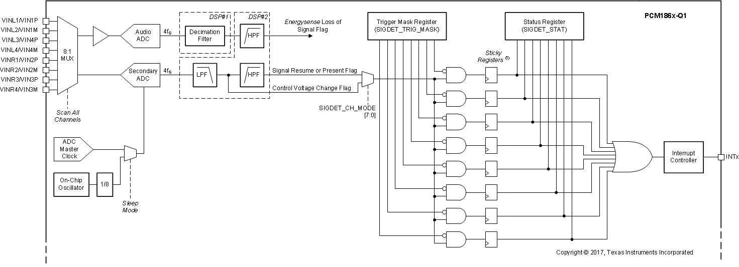
The secondary ADC has two main purposes in the PCM186x-Q1 family. The primary purpose is to act as a low power signal detection system, to aid with system wakeup from sleep. TI calls this functionality energysense. Other functionality includes the ability to use any spare analog inputs as generic ADC inputs, for connection to simple analog sources, such as voltages from control potentiometers. TI calls this functionality controlsense or dc control.
The secondary ADC is a one-bit, delta-sigma type ADC. The sampling rate is directly connected to the main ADC audio sampling clocks during ACTIVE functionality. When the device is in sleep state, then the secondary ADC switches the clock source to an on-chip oscillator (if there are no other clock sources).
In sleep mode, the inputs are all treated as single-ended inputs. Differential inputs are not supported in this mode because the PGA must be powered up, and thus, consume more power.
In active mode, energysense audio signal detection on any channels other than the primary is not available; however, other inputs can be read using the secondary ADC channel driven in controlsense mode.
In sleep mode, each input pin can be configured to perform either energysense or controlsense. Both functions can generate interrupts when their thresholds are crossed. All inputs will be cycled through and converted continuously, performing either an enerysense or a controlsense function.
In active mode, any dc based controls will either need to be polled continuously by the systems host, or streamed out continuously in a 6ch TDM mode. In an application, this may mean that the main input is being converted, while the system battery level, or analog volume control knob position is polled using controlsense.
To make the secondary ADC as flexible as possible in both energysense and controlsense modes, the following controls and coefficients are available in the register map. More details on each are in the relevant following sections.
- Coefficients for the secondary ADC low-pass filter
- Coefficients for the secondary ADC high-pass filter
- Reference voltage and interrupt voltage delta for each input in controlsense mode
- Signal loss conditions (time and threshold)
- Signal resume conditions (threshold)
- Interrupt behavior (for example, ping every x ms if host does not clear)
- Scan time for each single ended input
9.3.10.2.1 Secondary ADC Analog Input Range
To match the dynamic range of the secondary ADC to an incoming line level signal, an overall attenuation is applied to the incoming signal. This attenuation is also present in controlsense mode. The impact of this is that the secondary ADC in controlsense mode can only detect control signals up to 4.3 V. Exact values will vary a small amount from device to device along with the gain error.
Input impedance of the secondary ADC is designed to be 20 kΩ.
9.3.10.2.2 Frequency Response of the Secondary ADC
The natural response of the secondary ADC is not flat by frequency. However, the frequency response can be flattened, so that all frequencies are equally sensitive to the energysense detector by modifying the LPF or HPF biquads in the DSP.
9.3.10.3 Secondary ADC Controlsense DC Level Change Detection
This function is used for external analog controls, such as potentiometers to set volume, tone control, or a sensor. The data for control sense has no high pass filter applied to it, even if the main audio path does have a HPF enabled.
AS shown in Figure 36, there are two parameters for the dc level change detection: reference level (REF_LEVEL) and difference level (DIFF_LEVEL). Each input pin (input 1 through 8) has a different reference and difference level.
 Figure 36. DC Detection Function
Users set a reference point, and a difference point. If the voltage at the control point crosses the difference point then an interrupt is driven from the device. This is useful for filtering out noise, as well as reducing the load on the host processor for controls that tend to be set and forget (such as volume).
The data from the secondary ADC can also be streamed out of the device in TDM form and directly from the I2C register map. AUXADC_DATA_CTRL (Page.0 0x58) is used to configure and check the status of the DC detector.
This feature (thresholds and interrupts) is available in both active and sleep modes. In sleep mode, the device automatically scans through each channel designated a controlsense input. In active mode, the scanning will need to be done manually by a host microcontroller by modifying the SEC_ADC_INPUT_SEL (Page.0, 0x0A) register.
Most applications requiring the use of a potentiometer for control can simply use the SIGDET_DC_LEVEL_CHx_x registers to read the 8-bit value. To enable the SIGDET_DC_LEVEL_CHx_x registers to work, then the DC_NOLATCH AUXADC_DATA_CTRL (Page.0, 0x58, B[7]) should be set to 1, and the appropriate input pins should be set to controlsense inputs SIGDET_CH_MODE (Page.0, 0x30)
Direct 16-bit two's compliment reads from the secondary ADC can be done using AUXADC_DATA_CTRL (Page.0, 0x58) includes a latch function that is used to read the data the secondary ADC on demand in 16-bit two's compliment format from registers 0x59 and 0x5A.
9.3.11 Energysense
Energysense functionality has been added to the PCM186x-Q1 to aid with auto-sleep and auto-wakeup for end equipment systems that are expected to be sold within the European Union. The latest Ecodesign legislation in Europe has demanded that products consume less than 500 mW in standby. Most off-the-shelf external power adaptors can consume 300 mW when idling, leaving the system with only 200 mW available. In many systems that require that almost everything be powered down in sleep mode after there is no more content to be played, and then to be powered back up when signal enters the system again.
Energysense is designed to work in collaboration with a microcontroller to trigger interrupts notifying the microcontroller to change the state of the PCM186x-Q1, and the rest of the board (for example, amplifiers, and so on). The PCM186x-Q1 does not automatically switch between sleep and wake modes.
Energysense is split into two functions: signal loss flag and signal resume flag. Both are available on the PCM186x-Q1 software-controlled devices. The PCM1860-Q1 and PCM1861-Q1 only support signal resume, as shown in Table 17. By default, the signal resume threshold is set at –57 dBFS. Signal resume (autowakeup) only functions when the device has been set to sleep.
Table 17. Energysense States
| MODE | PURPOSE | CONDITIONS | POSITIVE OUTCOME | WORST CASE |
|---|---|---|---|---|
| SLEEP (Signal Detect Mode) | Detect Input Signal and Wake up from SLEEP | BCK and LRCK stopped (not locked) or register Set. | Host Wakes and services interrupt (reads register) | Host Doesn't respond or start clocks. |
| Trigger Interrupt when input crosses above (threshold) | Host Starts BCK/LRCK. (Moving system to ACTIVE mode) or writes to register. | PCM186x-Q1 keeps triggering interrupts until host responds. | ||
| Trigger for 1ms every X seconds until clocks start (x=1 by default) | ||||
| ACTIVE (Signal Loss Mode) | Detect content below (threshold) over time | BCK and LRCK are currently running | System can choose to go to sleep or not. If not, reset interrupt | If system does not sleep, remain in Mode 2, and prompt every Y. |
| Assist system to sleep after audio inactivity (for example, Source is off, but speaker still on) | If no content above -(threshold) dB for Y minutes, drive interrupt. | If System decides to sleep, stop BCK/LRCK. This will move PCM186x-Q1 to SLEEP mode. | MCU will need to mask that interrupt. |
9.3.11.1 Energysense Signal Loss Flag
The main ADC constantly monitors the input signal level while in ACTIVE mode. Should the input level remain below a register defined threshold (for example –60 dB - Virtual Coefficient 0x2C, programmable through Page 1.) for a register defined amount of time (for example 1 minute - set by SIGDET_LOSS_TIME (Page.0, 0x33) ), an interrupt can be generated.
If the system MCU decides to move to sleep mode, the PCM186x-Q1 can be moved to SLEEP by stopping BCK/LRCK or using PWRDN_CTRL (Page.0, 0x70); see Table 17 for details.
If BCK and LRCK are stopped by the host after the interrupt, the device goes to the sleep state as shown in Figure 37. Otherwise, the interrupt continues for a few seconds, defined by SIGDET_INT_INTVL (Page.0, 0x36) unless the interrupt and timeout counter is reset.
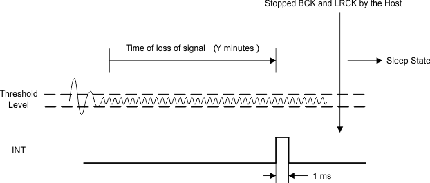 Figure 37. Energysense Signal Loss
In a typical application, the host MCU will note and reset this register multiple times until a system sleep number is hit. For example, a 5-minute signal loss could be implemented by using the default 1-minute timeout on the PCM186x-Q1, and counting five interrupts. An example is shown in Figure 38.
 Figure 38. Interrupt Behavior for Signal Loss
Alternatively, the SIGDET_LOSS_TIME (Page.0, 0x33) register in the device can be changed from one minute (default) to five minutes. This timeout is sample rate dependant. The expected sample rate is 48 kHz, but should the system be running at 96 kHz, then the time will be halved. (192 kHz = quarter the register setting).
The duration of the interrupt can also be modified using INT_PLS (Page.0 0x62) to be pulses, or to be a sticky flag, where sticky is defined as the interrupt is on until cleared.
9.3.11.2 Energysense Signal Detect Circuitry
In sleep mode (BCK and LRCK stop, or by register), the PCM186x-Q1 monitors the signal level or dc level change using the secondary ADC. All eight channels are converted one after the other in a circular manner. The scan time is specified with register SIGDET_SCAN_TIME. All eight channels are measured, even if some have the respective interrupt outputs muted. Accuracy and frequency response are a function of scan time. A long scan time allows detection of lower frequency content. The energysense signal wakeup logic is shown Figure 39.
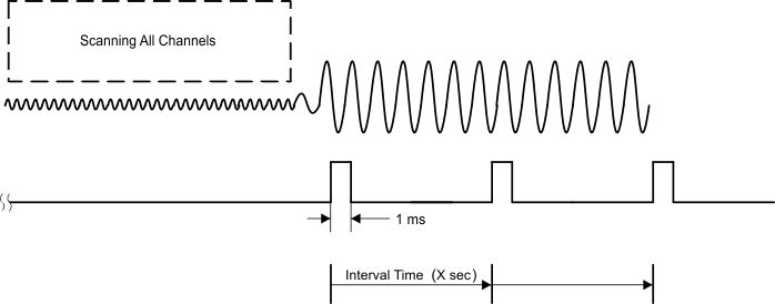 Figure 39. Energysense Signal Wakeup Logic
There is a balance between lowest frequency detectable, and time on that particular channel. There are three options in register SIGDET_INT_INTVL (Page.0 0x36):
- 50-Hz detect (160 ms per channel)
- 100-Hz detect (80 ms per channel)
- 200-Hz detect (40 ms per channel)
9.3.11.2.1 Energysense Threshold Levels for Both Signal Loss and Signal Detect
There are two threshold levels used for Energysense, as shown in Figure 40. One is the loss of signal level, another one is the resume of signal level.
 Figure 40. Dual Thresholds for Energysense
As both thresholds are DSP based, their coefficients are stored in virtual coefficient space that is programmed through the device register map.
For example, to change the resume threshold value to –30 dB (0x040C37):
Write 0x00 0x01 ; # change to register page 1
Write 0x02 0x2D ; # write the memory address of resume threshold
Write 0x04 0x04 ; # bit[23:15]
Write 0x05 0x0C ; # bit[15:8]
Write 0x06 0x37 ; # bit[7:0]
Write 0x01 0x01 ; # execute write operation
9.3.11.3 Programming Various Coefficients for Energysense
Programming the DSP coefficients for the energysense secondary ADC is done through the indirect virtual programming registers in Page1. The low-pass filter (LPF) and high-pass filter (HPF) coefficients can be written to flatten out the frequency response, as well as the energysense loss and resume thresholds. Visually, one can imagine the DSP flow as shown in Figure 41.
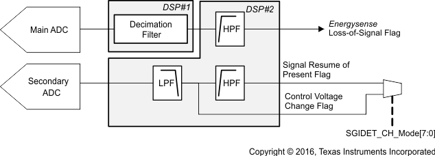 Figure 41. Energysense Process Flow
To flatten out the response of the secondary ADC, so that all frequencies are detected evenly, write the biquads shown in Table 18 to the virtual DSP memory, using the techniques discussed in the Programming DSP Coefficients on Software-Controlled Devices section.
Table 18. Secondary ADC Biquad Coefficients at 48-kHz Sampling
| COEFFICIENT | VIRTUAL RAM ADDRESS |
|---|---|
| LPF_B0 | 0x20 |
| LPF_B1 | 0x21 |
| LPF_B2 | 0x22 |
| LPF_A1 | 0x23 |
| LPF_A2 | 0x24 |
| HPF_B0 | 0x25 |
| HPF_B1 | 0x26 |
| HPF_B2 | 0x27 |
| HPF_A1 | 0x28 |
| HPF_A2 | 0x29 |
9.3.12 Audio Processing
Both DSP1 and DSP2 are fixed function processors that are not custom-programmable. They are used in this device to perform multiple filtering, mixing functions, signal detection and housekeeping functions. Programming the DSP coefficients is done indirectly using registers on Page1. The data and target DSP memory address are stored in registers, and once the DSPs are ready for the data (that is done by request) the data is then latched into the DSP memory.
This indirect method of programming the DSP allows multiple registers to be written, without consuming valuable register map space. More details can be found in the Programming DSP Coefficients on Software-Controlled Devices section.
9.3.12.1 DSP1 Processing Features
9.3.12.1.1 Digital Decimation Filters
The main audio path uses a selectable decimation filter used to convert the high-data-rate modulator to I2S rates. A choice between a classic FIR response and a low-latency IIR response is available. A high-pass filter, separate from that used for the secondary ADC, is also available to remove any dc bias that may be present in the signal. This feature is enabled by default.
Details can be found in the DSP_CTRL register (Page.0, 0x71).
9.3.12.1.2 Digital PGA
As discussed in the Programmable Gain Amplifier section, the digital PGA gain can be controlled by the auto gain mapping function, that will use the analog gain settings in register PGA_VAL_CH1_L (Page.0 0x01) and related registers to achieve the target gain with a combination of digital and analog gain. However, digital gain can be also controlled directly by disabling the auto gain mapping function using register PGA_CONTROL_MAPPING (Page.0 0x19). Manual update of digital PGA is only available in 4-channel devices because the digital PGA gain is fixed to 0 dB when manual gain mapping is enabled.
9.3.12.2 DSP2 Processing Features
9.3.12.2.1 Digital Mixing Function
This function allows post ADC mixing, as well as ADC + incoming I2S mix. Volume control functionality can be performed prior to outputting the signal to an I2S DAC or Amplifier.
Gain range is from –120 dB to +18 dB (4.20 format). Phase Inversion can be done by performing the two's compliment of the positive gain coefficient. two's compliment can be performed by inverting all bits in the binary coefficient, and adding 1 to the LSB.
As the DSP coefficients are directly written, no soft ramping is available. Use of I2S receive sacrifices two digital mic channels due to pin limitations.
Coefficients are written indirectly to virtual memory addresses using the registers on page 1. Details of the registers are shown in the Register Map section.
A diagram of the digital mixing functionality is shown in Figure 42.
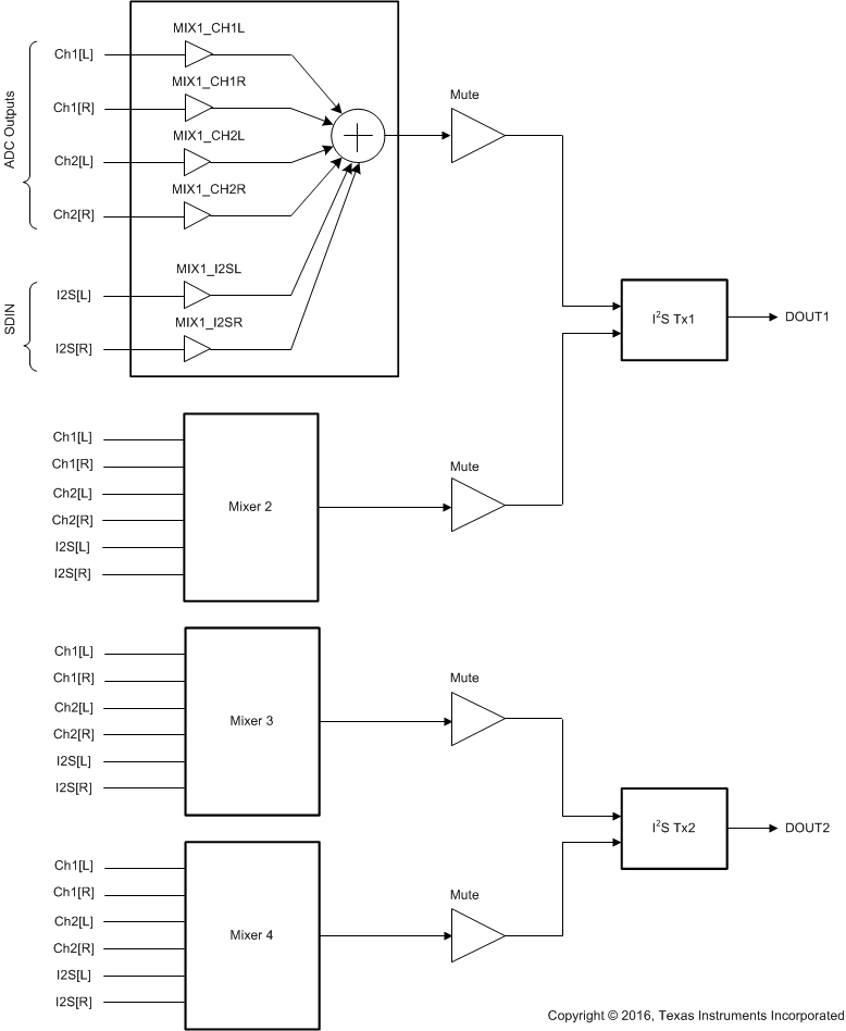 Figure 42. Digital Mixer Functionality
9.3.13 Fade-In and Fade-Out Functions
The PCM186x-Q1 has fade-in and fade-out functions on DOUT to avoid pop noise. This function is engaged on device power up or down, and mute or unmute. The level changes from 0 dB to mute, or mute to 0 dB, are performed using pseudo S-shaped characteristics calculation with zero-cross detection. Because of the zero-cross detection, the time needed for the fade-in and fade-out depends upon the analog input frequency (fIN). Fade takes 48 / fIN until processing is completed. If there is no zero cross during 8192 / fS, DOUT is faded in or out by force during 48 /fS (TIME OUT). Figure 43 illustrates the fade-in and fade-out operation processing.
 Figure 43. Fade-In and Fade-Out Operations
9.3.14 Mappable GPIO Pins
All the GPIO pins on thePCM186x-Q1 software-controlled devices can be configured for various functions. They can each have their polarity inverted to make control of following circuits easier. See the control registers for each GPIO for a better explanation of mapping. (such as GPIO1_FUNC at Page.0 0x10)
The type of function can also be controlled, including such behavior as regular inputs, inputs with toggle detection, or sticky bits. The device can also be configured as an open drain output, so that multiple interrupt outputs from different devices in the system can be connected together.
9.3.15 Interrupt Controller
The hardware-controlled PCM1860-Q1 and PCM1861-Q1 has the energysense signal detect as the default output on the INT pin. There are no other interrupt sources. The INT pin on the PCM1860-Q1 and PCM1861-Q1 is also used to put the device into power-down mode. Figure 44 shows the interrupt logic
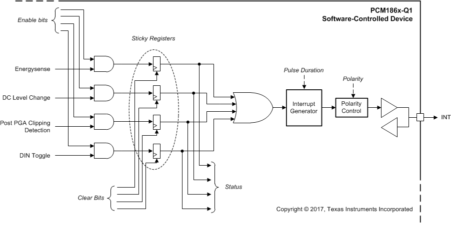 Figure 44. Interrupt Logic
The software-controlled devices have multiple signals that can be mapped to the interrupt outputs. These include:
- Energysense (default)
- Secondary ADC controlsense interrupt
- Post PGA clip
- DIN toggle
The Interrupt controller has the following features
- The Interrupt sources can be filtered by the enable register (INT_EN).
- The Interrupt flags can be monitored by reading the status register (INT_STAT).
- The interrupt flags can be cleared by writing the status register.
- The polarity of the interrupt signal can be changed between active high, active low and Open Collector (High Impedance is pulled to GND) (INT_PLS).
- The pulse width of the interrupt signal can be changed between 1ms, 2ms, 3ms and 4ms.
- The interrupt controlled cannot remain asserted, the status bits can be sticky, but the interrupt pin itself has no hold function.
Using a combination of these features, as well as the interrupt sources, allows the PCM186x-Q1 to alert a host microcontroller of an event, using whichever polarity signal required (pull high, pull low, Hi-Z open collector). The host controller can then communicate with the device to poll the interrupt flag register to find out what happened. Additional registers can then be read for more details. (For instance, which input triggered an energysense event.). From a register point of view, there is no difference between INT A, INT B and INT C logic, other than their signaling (positive, negative or open drain).
9.3.15.1 DIN Toggle Detection
DIN toggle can be used to trigger from an external PCM audio data source or any other digital data source (such as a IR remote control UART stream) where there is a toggling logic state. (from 0 V to 3.3 V, or vice versa). All GPIO pins support DIN toggle detection, other than GPIO2.
This function is only enabled in sleep mode.
9.3.15.2 Clearing Interrupts
Each Interrupt type has a specific method to clear. When clearing or resetting an interrupt, always remove the source of the interrupt first.
9.3.15.2.1 Reset Energysense Loss (in Active Mode)
Background: In active mode, the threshold is set to a system-level defined loss threshold (for example, –80 dBFS), and the timeout set to 1 minute.
After 1 minute, the interrupt triggers. To reset energysense loss, take the following steps:
Step 1: Disable the interrupt in INT_EN (Page.0 0x60)
Step 2: Look at INT_STAT (Page.0 0x61). What is the energysense interrupt?
The interrupt status register INT_STAT (Page.0 0x61) is sticky in active mode. After being set, this register cannot be reset without clearing SIGDET_STAT (Page.0 0x32).
Step 3 Option 1:The easiest way to clear the register is to move to sleep mode. PWRDN_CTRL (Page.0 0x70)
Step 3 Option 2: To ignore the interrupt, or to clear it and remain in active mode (and wait another minute)
Step 4: Set the signal loss threshold to –110 dB (so that the interrupt is no longer generated by internal logic)
Step 5: Clear the SIGDET_STAT (Page.0 0x32) register by:
Write 0xFF to SIGDET_STAT (Page.0 0x32)
Read SIGDET_STAT (Page.0 0x32). The register should be 0x00
Step 6: Now set signal loss threshold to the original –80 dBFS
Step 7: Enable the interrupt again INT_EN (Page.0 0x60)
9.3.15.2.2 Reset Energysense Detect (In Sleep Mode)
Background: The device is in sleep mode, with the wake threshold set as a DSP memory coefficient.
INT_STAT (Page.0 0x61) is sticky and SIGDET_STAT (Page.0 0x32) is not sticky in this mode. The Interrupt pin triggers dynamically as the audio crosses the threshold. The SIGDET_STAT (Page.0 0x32) register shows which input is causing the input only while that particular input is causing the interrupt. The INT_STAT (Page.0 0x61) register shows the energysense interrupt has been triggered until it is cleared.
The system host controller responds to the interrupt in one of two ways:
Option 1: Move to active mode. PWRDN_CTRL (Page.0 0x70)
Option 2: Ignore the interrupt in the system controller, or disable the interrupt for a set amount of time using INT_EN (Page.0 0x60)
9.3.15.2.3 Reset Controlsense (Active and Sleep Modes)
If a potentiometer has been moved and the interrupt asserts, the following steps should be taken:
Step 1: Read the INT_STAT (Page.0 0x61) to confirm it is a controlsense event.
Step 2: Disable the controlsense interrupt temporarily: INT_EN (Page.0 0x60)
Step 3: Read the SIGDET_STAT (Page.0 0x32) to see which channel changed
Step 4: Read the appropriate SIGDET_DC_LEVEL_CHx_x to find the new value
Step 5: Copy the value to the appropriate SIGDET_DC_REF_CHx_x register. This action should stop the interrupt being caused internally.
Step 6: Re-enable the Interrupt INT_EN (Page.0 0x60)
9.3.15.2.4 Reset DIN Toggle (In Sleep Mode)
Background: The DIN toggle mode can detect if there is a toggle on an external data pin. For The INT pin will pulse as and when the Internal ADC flow clips. Despite the dynamic nature of the interrupt output pin, INT_STAT (Page.0 0x61) is a sticky register. To clear this register, take the following steps:
Step 1: Read the INT_STAT (Page.0 0x61) to confirm it is a PGA clipping event.
Step 2: Lower the gain of the current input channel INT_EN (Page.0 0x60)
Step 3: Reset the interrupt using INT_EN (Page.0 0x60). Set bit 5 to 0, then back to 1
Step 4: Bit 5 of INT_STAT (Page.0 0x61) should now be 0. If not, go to step 2 again.
9.3.15.2.5 Reset PGA Clipping (Active)
Background: PGA Clipping is a dynamic interrupt. The INT pin will pulse as and when the Internal ADC flow clips. Despite the dynamic nature of the interrupt output pin, INT_STAT (Page.0 0x61) is a sticky register. To clear this register, take the following steps:
Step 1: Read the INT_STAT (Page.0 0x61) to confirm it is a PGA clipping event.
Step 2: Lower the gain of the current input channel INT_EN (Page.0 0x60)
Step 3: Reset the interrupt using INT_EN (Page.0 0x60). Set bit 5 to 0, then back to 1.
Step 4: Bit 5 of INT_STAT (Page.0 0x61) should now be 0. If not, go to step 2 again.
9.3.16 Audio Format Selection and Timing Details
9.3.16.1 Audio Format Selection
Format selection for the PCM1860-Q1 and PCM1861-Q1 is controlled using a hardware pin configuration. There is a choice of left-justified data (known as LJ) or I2S.
On the PCM186x-Q1 software-controlled devices, format selection is done with the registers in I2S_FMT (Page.0 0x0B), which offers additional support for right-justified (RJ) and time division multiplexed (TDM) data for multiple channels.
The PCM186x-Q1 software-controlled devices also offer an additional DOUT pin that can be driven through the GPIO pins. For an example, see the register details at GPIO1_FUNC (Page.0 0x10).
9.3.16.2 Serial Audio Interface Timing Details
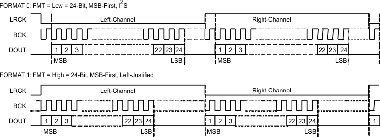 Figure 45. Audio Data Format
 (LRCK and BCK Work as Inputs in Slave Mode and as Outputs in Master Mode)
9.3.16.3 Digital Audio Output 2 Configuration
The PCM186x-Q1 four-channel software-controlled devices offer an additional DOUT through the use of a GPIO that has its rate synchronized with the primary DOUT. DOUT2 is configured using the digital mixer, shown in Digital Mixing Function. In TDM Modes, DOUT2 is not available.
The GPIO used for DOUT2 can be set using registers. GPIO0 is used for SPI-MOSI in SPI mode, however, it can be retasked for DOUT2 duties if MOSI is not required.GPIO0_FUNC (Page.0 0x10), GPIO1_FUNC (Page.0 0x10), GPIO2_FUNC (Page.0 0x11), or GPIO3_FUNC (Page.0 0x11) can be used to set GPIOx to DOUT2
9.3.16.4 Time Division Multiplex (TDM Support)
The software-controlled devices can support TDM for both slave and master modes. In many devices, this is also known as DSP Mode.
Data on the TDM stream can be between two and four channels of audio content from each PCM186x-Q1 mixer output. By default, each mixer passes data from the respective ADC in a bypass or passthrough configuration. Data from the secondary ADC can also be output on channels five and six. The frame rate in TDM mode fixed to 256 BCK per frame, and the duty cycle of the LRCK (or frame sync signal) can be either a 50 / 50 duty cycle, or a single bit at the start of the frame.
Up to 32 bits per channel are available. In 32-bit mode, 24 bits of data and 8 bits of padding (zero) are used per channel. In 24-, 20-, and 16-bit data, no padding is provided between channels. In 24-bit mode, channel two begins transmitting on bit clock 25.
In data formats lower than 24 bits, the data is simply truncated, not dithered to 16 bits.
In slave mode, only a rising edge on the first bit is required to start the frame. (similar to MSB-first, left-justified).
In master mode, only a 50% duty cycle on the output is possible. This configuration is made by setting TDM_LRCK_MODE (Page.0 0x0B) to 0.
Typically when interfacing to a DSP, only the rising edge on the first bit of data of the frame is required.
While the device is not transmitting data (but still being clocked), the DOUT pin will be Hi-Z (high impedance) to allow other devices on the bus to transmit their data.
TDM mode is configured using I2S_FMT (Page.0 0x0B), TDM_LRCK_MODE (Page.0 0x0B), TDM_OSEL (Page.0 0x0C)
The timing limits for the interface signals are defined by the Serial Audio Data Interface Configuration section with the addition that the BCK period minimum must at least 1 / (512 × fS) to ensure that data is clocked in correctly.
The audio format is shown below. The 24-bit data can fit up to 10 channels of data in a 256x bitclock stream; however, the I2C-controlled devices only have two possible I2C addresses. The eight channels of audio data should be no issue.
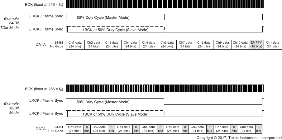 Figure 46. Audio Format for TDM
NOTE
TDM mode can only function up to 96 kHz sampling rate when IOVDD is 1.8 V. This is due to an I/O limitation of 25 MHz at 1.8 V.
9.3.16.5 Decimation Filter Select
The PCM186x-Q1 offers a choice of two different digital filters, a Classic FIR response and a low latency IIR.
9.3.16.6 Serial Audio Data Interface Configuration
The PCM186x-Q1 devices interface to the audio system through LRCK, BCK and DOUT.
The PCM186x-Q1 hardware-controlled devices are configured using pin MD4 to select between left-justified data and I2S.
The PCM186x-Q1 software-controlled devices are configured using register I2S_FMT (Page.0 0x0B). Use register I2S_TX_OFFSET (Page.0 0x0D) when dealing with TDM systems to offset the data transmit.
In addition, the offset required for receiving 24-bit data is programmed using RX_TDM_OFFSET (P0, R0x0E).
9.4 Device Functional Modes
9.4.1 Power Mode Descriptions
The PCM186x-Q1 family has multiple power modes: active, sleep, idle, and standby. Table 19 lists the power modes and functions.
- Active mode: describes the mode where the device is targeting full performance and functionality.
- Idle mode: describes the mode where the digital output is muted and the analog side (such as PGAs) are still powered up.
- Sleep mode: describes the mode where the main ADCs are not in use, but the device continues to do Energysense input level detection.
- Standby mode: drops the power into an ultra-low power mode where only the control port is available.
Table 19. Power Modes
| FUNCTIONS | ACTIVE OR IDLE (MUTE) | SLEEP (Energysense) | STANDBY |
|---|---|---|---|
| ANALOG FUNCTIONS | |||
| Programmable Gain Amps | ON | OFF | OFF |
| ADC | ON | OFF | OFF |
| ADC Reference | ON | OFF | OFF |
| CMBF | ON | ON | ON |
| Reference | ON | ON | ON |
| Mic Bias | ON | ON | OFF |
| Secondary ADC PGA | ON | ON | OFF |
| Secondary PGA | ON | ON | OFF |
| ACCESSORY FUNCTIONS | |||
| LDO | ON | ON | ON |
| Oscillator | ON | ON | ON |
| Clock Halt Detection | ON | ON | ON |
| PLL | ON | ON | OFF |
| Digital Cores | ON | 20% ON | 5% ON (Control Port Only) |
9.4.1.1 PCM1860-Q1 and PCM1861-Q1 Hardware Device Power Down Functions
9.4.1.1.1 Enter Standby Mode (From Active Mode)
The external host should drive the INT pin (GPIO3) high (whilst there is no interrupt pending) to place the device in Idle mode.
The INT pin is configured as an energysense interrupt output on the hardware-controlled device; therefore, the external host microcontroller should use it as multi-function pin. (MCU pin configured as INPUT when no requirement exists to move to standby, MCU pin as OUTPUT driving HIGH when a need exists to place the device in an idle state.)
NOTE
While the device is driving its interrupt high, any external voltage on the INT pin will be ignored by the device, until the interrupt event (and pulse) is finished.
9.4.1.1.2 Exit From Standby Mode Back to Active
The external MCU host releases the INT pin (GPIO3). This typically involves reconfiguring the external MCU GPIO into an INPUT or HI-Z.
9.4.1.1.3 Enter or Exit Sleep or Energysense Mode to Active
Enter sleep mode: Halt BCK and LRCK
Exit sleep mode: Resume BCK and LRCK
9.4.1.2 PCM186x-Q1 Software Device Power Down Functions
9.4.1.2.1 Enter or Exit Stand-by Mode
Enter standby mode: Send power down command by writing register PWRDN_CTRL (Page.0 0x70)
Exit standby mode: Send power up command by writing register PWRDN_CTRL (Page.0 0x70)
9.4.1.2.2 Enter Sleep Mode
Send sleep command by writing register PWRDN_CTRL (Page.0 0x70) or
Halt BCK and LRCK when I2S is configured as I2S slave mode
9.4.1.2.3 Exit Sleep Mode
Send resume from (exit) sleep command by writing register PWRDN_CTRL (Page.0 0x70) or
Resume BCK and LRCK when I2S is configured as I2S slave mode
9.4.1.3 Bypassing the Internal LDO to Reduce Power Consumption
The PCM186x-Q1 has an integrated LDO allowing single 3.3-V supply operation. However, developers desiring to minimize power consumption can bypass the on-chip LDO and provide 1.8 V to IOVDD and to LDO under the following conditions:
- TDM mode is limited to BCK driving a maximum of 25 MHz, because the BCK and DATA cells cannot exceed 25 MHz when IOVDD is 1.8 V. Consequently, a maximum of 96-kHz sampling frequency operation is possible.
- IOVDD MUST be 1.8 V along with LDO, if an external 1.8 V supply is used to bypass the internal LDO.
9.5 Programming
9.5.1 Control
9.5.1.1 Hardware Control Configuration
PCM186x-Q1 devices require the following functions to be configured on startup. Hardware-controlled devices require a subset of these configurations:
- Control interface type and address for PCM186x-Q1 software-controlled devices
- The clock mode and rate (automatic in slave mode, or divider ratio in master mode) for hardware-controlled devices. For more details see the Clocks section.
- The interface audio data format for hardware-controlled devices.
- Digital filter selection (FIR or IIR) for hardware-controlled devices; requires a power cycle to change.
- Analog input channels and PGA gain for hardware-controlled devices.
9.5.1.2 Software-Controlled Device Configuration
PCM186x-Q1 software-controlled devices are configured and controlled by using either I2C or SPI using MD0 and MD1. Table 20 shows the MD0 control protocols, and Table 21 shows the MD1 mode selection.
Table 20. MD0: Control Protocol Select
| MD0 | Control Protocol |
|---|---|
| Low (or floating) | I2C Mode |
| High | SPI Mode |
Table 21. MD1: I2C Address or SPI Chip Select
| MODE | MD1 USE | STATIC MD1 VALUE | CONFIGURATION |
|---|---|---|---|
| I2C | Address pin | Low | I2C Address: 0x94 |
| I2C | Address pin | High | I2C Address: 0x96 |
| SPI | MS (SPI Chip Select) | N/A | N/A |
9.5.1.3 SPI Interface
The SPI interface is a 4-wire synchronous serial port that operates asynchronously to the serial audio interface and the system clock (SCK). The serial control interface is used to program and read the on-chip mode registers.
The control interface includes MISO, MOSI, MC, and MS. MISO (master in slave out) is the serial data output, used to read back the values of the mode registers; MOSI (master out slave in) is the serial data input, used to program the mode registers.
MC is the serial bit clock, used to shift data in and out of the control port on the MC falling edge. MS is the active-low mode control enable, used to enable the internal mode register access. If data from the device is not required, the MISO pin can be assigned to GPIO1 by register control.
9.5.1.3.1 Register Read and Write Operation
All read and write operations for the serial control port use 16-bit data words. Figure 47 shows the control data word format. The most significant bit is the read and write (R/W) bit. For write operations, the bit must be set to 0. For read operations, the bit must be set to 1. There are seven bits, labeled IDX[6:0], that hold the register index (or address) for the read and write operations. The least significant eight bits, D[7:0], contain the data to be written to, or the data that was read from, the register specified by IDX[6:0].
Figure 48 and Figure 49 show the functional timing diagram for writing or reading through the serial control port. MS should be held at logic 1 state until a register needs to be written or read. To start the register write or read cycle, MS should be set to logic 0. Sixteen clocks are then provided on MC, corresponding to the 16 bits of the control data word on MOSI and readback data on MISO. After the eighth clock cycle has completed, the data from the indexed-mode control register appears on MISO during the read operation. After the sixteenth clock cycle has completed, the data is latched into the indexed-mode control register during the write operation. To write or read subsequent data, MS should be set to logic 1 once.

NOTE:
B8 is used for selection of write or read. Setting = 0 indicates a write, while = 1 indicates a read. Bits 15–9 are used for register address. Bits 7–0 are used for register data. Figure 48. Serial Control Format for Write
 Figure 49. Serial Control Format for Read
9.5.1.4 I2C Interface
The PCM186x-Q1 software-controlled devices support the I2C serial bus and the data transmission protocol for standard and fast mode as a slave device. This protocol is explained in I2C specification 2.0.
The I2C control port is available even in the absence of any other clocks in the system.
In I2C mode, the control pins are changed as shown in Table 22.
Table 22. I2C Pins and Functions
| PIN NAME | PIN NUMBER | PROPERTY | DESCRIPTION |
|---|---|---|---|
| SDA | 23 | Input / Output | I2C data |
| SCL | 24 | Input | I2C clock |
| AD | 25 | Input | I2C address 1 |
9.5.1.4.1 Slave Address
The PCM186x-Q1 software-controlled devices have a 7-bit slave address, as shown in Table 1. The first six bits (MSBs) of the slave address are factory preset to 1001 01. The next bit of the address byte is the device select bit, which can be user-defined by the AD pin. A maximum of two PCM186x-Q1 devices can be connected on the same bus at one time. Each device responds when receiving the respective slave address.
Table 1. I2C Slave Address
| MSB | LSB |
| 1 | 0 | 0 | 1 | 0 | 1 | AD | R/W |
9.5.1.4.2 Packet Protocol
A master device must control packet protocol, which consists of start condition, slave address, read/write bit, data if write or acknowledge if read, and stop condition. The PCM186x-Q1 software-controlled devices support only slave receivers and slave transmitters. Figure 50 shows the basic I2C framework.
 |
|||||||||||
| write operation |
| Transmitter | M | M | M | S | M | S | M | S | ------------ | S | M |
| Data Type | St | slave address | R/W | ACK | DATA | ACK | DATA | ACK | ACK | Sp |
| read operation | |||||||||||
| Transmitter | M | M | M | S | M | S | M | S | ------------ | S | M |
| Data Type | St | slave address | R/W | ACK | DATA | ACK | DATA | ACK | ACK | Sp |
| M: Master Device MMM S: Slave Device | |||||||||||
| St: Start Condition MMM Sp: Stop Conditiion | |||||||||||
9.5.2 Current Status Registers
Page.0, registers 0x72 through 0x75 and 0x78 can be used to read the device status at any time. Sample rate, power rail status, clock error, and clock ratios can all be read from these registers.
9.5.3 Real World Software Configuration using Energysense and Controlsense
To gain the benefit of many of the PCM186x-Q1 features, use a microcontroller to monitor and control the device. There are two main modes withing the device, Active and Sleep. Using a microcontroller to process the interrupts for both energysense and controlsense allows the system to intelligently wake and sleep as well as update system controls. Figure 51 and Figure 52 show flow diagrams for both active and sleep modes, respectively. Extended I2C register settings are shown in Bold Text.
9.5.3.1 Active Mode Flow Diagram
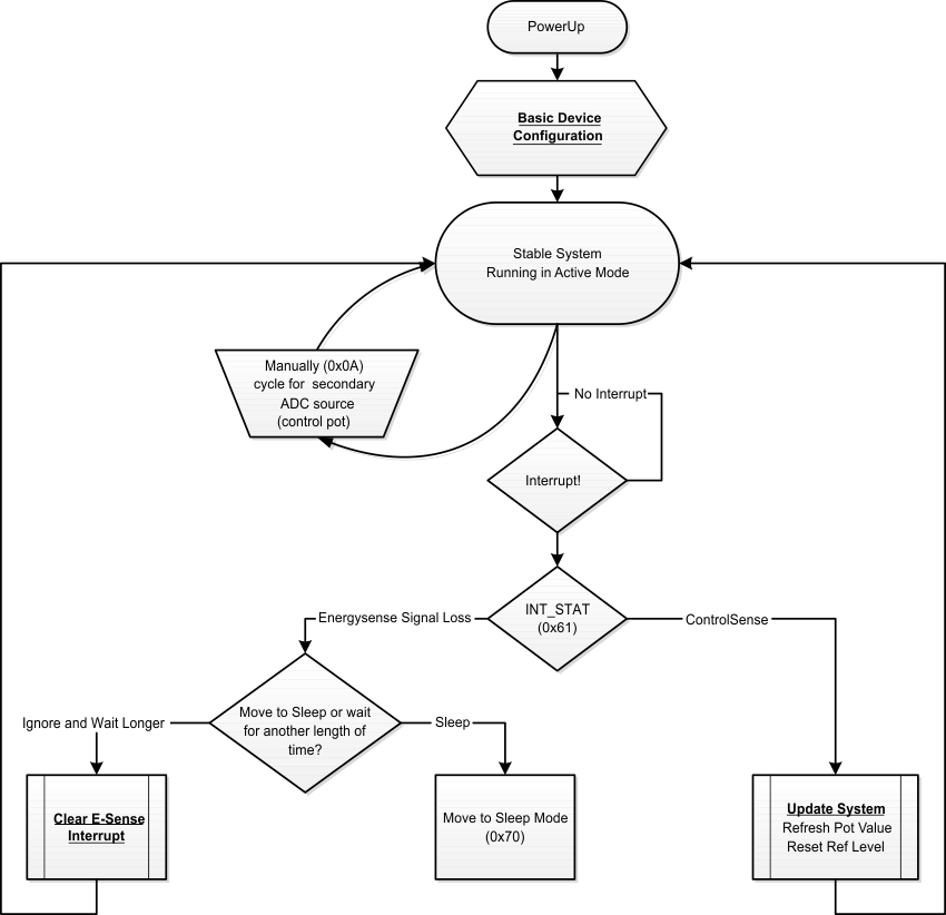 Figure 51. Active Mode Flow Chart
9.5.3.2 Basic Device Configuration
The device by default starts in slave mode at 48 kHz (per the EVM)
Set global loss level to be –50 dB using the DSP coefficient method.
Set 4R as controlsense input (for example, a control voltage for volume control) using SIGDET_CH_MODE (0x30)
Configure active mode secondary to be channel 4R using SEC_ADC_INPUT_SEL (0x0A)
Set Read Data without latch in register AUXADC_DATA_CTRL (0x58)
Set interrupts (energysense and controlsense) using INT_EN (0x60)
Set interrupt pulse for 3 mS (makes it easier to see it visually using INT_PLS (0x62)
9.5.3.3 Clear Energysense Interrupt
Disable the energysense interrupt in INT_STAT register (0x61)
Remove the interrupt source by changing the loss detect threshold to 110 dB (ADC noise level) using the DSP coefficient method.
Write 0xFF to the SIGDET_STAT (0x32) register.
Write 0x00 to the SIGDET_STAT (0x32) register.
Change the loss detect threshold back to –50 dB using the DSP coefficient method.
Re-enable the energysense interrupt in INT_STAT register (0x61)
9.5.3.4 Update System Settings
Read interrupt status INT_STAT register(0x61)
Clear interrupt enable INT_EN (0x60)
Check which input caused the interrupt; in this case, looking for (4R) SIGDET_STAT (0x32)
Read new 4R data (for example, SIGDET_DC_LEVEL_CH4_R 0x57).
Host would normally process as needed. (foe example, change volume in the amplifier)
Set SIGDET_DC_REF_CH4_R (0x55) to be the new value.
Now that interrupt source is removed, we can clear the SIGDET_STAT register (0x32)
Write 0xFF to SIGDET_STAT register (0x32).
Write 0x00 to SIGDET_STAT register (0x32).
Re-enable control Sense Interrupt in INT_EN (0x60)
9.5.3.5 Sleep Mode Flow Diagram
The sleep mode flow chart is shown in Figure 52.
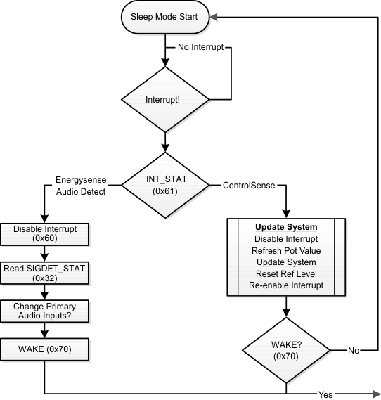 Figure 52. Sleep Mode Flow Chart
9.5.3.6 Update Controlsense values in Sleep Mode
9.5.3.6.1 Update System Settings
In sleep mode, any channels set as controlsense inputs are scanned through automatically. The read and writes to SIGDET_DC_REF_CHx_x and SIGDET_DC_LEVEL_CHx_x should be selected based on whichever input caused the interrupt.
Read interrupt status INT_STAT register(0x61)
Clear controlsense interrupt enable INT_EN (0x60)
Check which input caused the interrupt SIGDET_STAT (0x32)
Read new data (for example, SIGDET_DC_LEVEL_CHx_x).
Host would normally process as needed (for example, change volume in the amplifier)
Set SIGDET_DC_REF_CHx_x to be the new value.
Now that interrupt source is removed, we can clear the SIGDET_STAT register (0x32) --
Write 0xFF to SIGDET_STAT register (0x32).
Write 0x00 to SIGDET_STAT register (0x32).
Re-enable controlsense interrupt in INT_EN (0x60)
9.5.4 Programming and Register Reference
9.5.4.1 Coefficient Data Formats
All mixer gain coefficients are 24-bit coefficients using a 4.20 number format. Numbers formatted as 4.20 numbers have 4 bits to the left of the binary point and 20 bits to the right of the binary point.
The most significant bit of the 4.20 number format is the sine bit. It is used, as part of a two's complement number to invert the phase of that mixer input.
See SLAC663 for a calculator to convert from dB to the hexadecimal coefficient required.
9.5.5 Programming DSP Coefficients on Software-Controlled Devices
The two fixed function DSPs on chip can have coefficients for filters and mixers programmed to them. This is done indirectly using specific registers on page 1. The devices integrate a memory arbiter that copies the coefficient from the I2C or SPI register space to the appropriate DSP memory address, when the DSP has completed its instructions for that sample. The refresh mechanism for the memory arbiter to update the I2C or SPI register space requires two dummy I2C writes to move from the DSP internal memory, through the arbiter and onwards to be visible in the I2C or SPI register space. See Figure 53
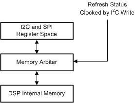 Figure 53. Register to DSP Memory Structure
Each 24-bit coefficient can be written once every audio sample. This allows a single sample update of a mixer coefficient, however, biquad coefficients will require multiple audio samples for all of the coefficients to be written. Under such conditions, the device should be muted until all coefficients are written. Otherwise, the biquad could become unstable.
In addition, DSP Internal memory can only be written to when the DSP is provided a clock from either the PLL or an external master clock source. Requesting a WREQ = 1 Register 0x01 of page 0x01 will have no effect, if the DSP is not currently running. This is of relevance if the system is running as a clock slave, and the clocks stop.
For example, to write to these registers, change the energysense resume threshold value to –30 dB (0x040C37)
- Write 0x00 0x01 ; # change to register bank 1
- Write 0x00 0x01 ; # two dummy writes to update the status of the write busy bit
- Write 0x00 0x01 ; # ^^^^
- Read Register 0x01 # if value is 0x00 then continue (check if system is still writing/reading). Otherwise, do another dummy write and check again.
- Write 0x02 0x2D ; # write the memory address of resume threshold
- Write 0x04 0x04 ; # bit[23:15]
- Write 0x05 0x0C ; # bit[15:8]
- Write 0x06 0x37 ; # bit[7:0]
- Write 0x01 0x01 ; # execute write operation
See SLAC663 for more details.
The internal DSP coefficient memory space is mapped as shown in Table 23.
Table 23. Virtual 24-Bit DSP Coefficient Registers
| NAME | COEFFICIENT | ADDRESS | DESCRIPTION |
|---|---|---|---|
| Mixer-1 | MIX1_CH1L | 0x00 | 4.20 format |
| MIX1_CH1R | 0x01 | ||
| MIX1_CH2L | 0x02 | ||
| MIX1_CH2R | 0x03 | ||
| MIX1_I2SL | 0x04 | ||
| MIX1_I2SR | 0x05 | ||
| Mixer-2 | MIX2_CH1L | 0x06 | 4.20 format |
| MIX2_CH1R | 0x07 | ||
| MIX2_CH2L | 0x08 | ||
| MIX2_CH2R | 0x09 | ||
| MIX2_I2SL | 0x0A | ||
| MIX2_I2SR | 0x0B | ||
| Mixer-3 | MIX3_CH1L | 0x0C | 4.20 format |
| MIX3_CH1R | 0x0D | ||
| MIX3_CH2L | 0x0E | ||
| MIX3_CH2R | 0x0F | ||
| MIX3_I2SL | 0x10 | ||
| MIX3_I2SR | 0x11 | ||
| Mixer-4 | MIX4_CH1L | 0x12 | 4.20 format |
| MIX4_CH1R | 0x13 | ||
| MIX4_CH2L | 0x14 | ||
| MIX4_CH2R | 0x15 | ||
| MIX4_I2SL | 0x16 | ||
| MIX4_I2SR | 0x17 | ||
| Secondary ADC LPF and HPF Coefficients | LPF_B0 | 0x20 | 1.23 format |
| LPF_B1 | 0x21 | ||
| LPF_B2 | 0x22 | ||
| LPF_A1 | 0x23 | ||
| LPF_A2 | 0x24 | ||
| HPF_B0 | 0x25 | ||
| HPF_B1 | 0x26 | ||
| HPF_B2 | 0x27 | ||
| HPF_A1 | 0x28 | ||
| HPF_A2 | 0x29 | ||
| Energysense | Loss_threshold | 0x2C | 1.23 format |
| Resume_threshold | 0x2D |
