SBOS424C March 2008 – November 2015 PGA112 , PGA113 , PGA116 , PGA117
PRODUCTION DATA.
- 1 Features
- 2 Applications
- 3 Description
- 4 Revision History
- 5 Device Comparison
- 6 Pin Configuration and Functions
- 7 Specifications
- 8 Detailed Description
-
9 Applications and Implementation
- 9.1
Application Information
- 9.1.1 Op Amp: Input Stage
- 9.1.2 Op Amp: General Gain Equations
- 9.1.3 Op Amp: Frequency Response Versus Gain
- 9.1.4 Analog MUX
- 9.1.5 System Calibration Using The PGA
- 9.1.6 Driving and Interfacing to ADCs
- 9.1.7 Power Supplies
- 9.1.8 Shutdown and Power-On-Reset (POR)
- 9.1.9 Typical Connections: PGA116, PGA117 (TSSOP-20)
- 9.2 Typical Applications
- 9.1
Application Information
- 10Power Supply Recommendations
- 11Layout
- 12Device and Documentation Support
- 13Mechanical, Packaging, and Orderable Information
Package Options
Refer to the PDF data sheet for device specific package drawings
Mechanical Data (Package|Pins)
- DGS|10
Thermal pad, mechanical data (Package|Pins)
Orderable Information
1 Features
- Rail-to-Rail Input and Output
- Offset: 25 μV (Typical), 100 μV (Maximum)
- Zerø Drift: 0.35 μV/°C (Typical), 1.2 μV/°C (Maximum)
- Low Noise: 12 nV/√Hz
- Input Offset Current: ±5 nA Maximum (25°C)
- Gain Error: 0.1% Maximum (G ≤ 32),
0.3% Maximum (G > 32) - Binary Gains: 1, 2, 4, 8, 16, 32, 64, 128 (PGA112, PGA116)
- Scope Gains: 1, 2, 5, 10, 20, 50, 100, 200 (PGA113, PGA117)
- Gain Switching Time: 200 ns
- 2 Channel MUX: PGA112, PGA113
10 Channel MUX: PGA116, PGA117 - Four Internal Calibration Channels
- Amplifier Optimized for Driving CDAC ADCs
- Output Swing: 50 mV to Supply Rails
- AVDD and DVDD for Mixed Voltage Systems
- IQ = 1.1 mA (Typical)
- Software and Hardware Shutdown: IQ ≤ 4 μA (Typical)
- Temperature Range: –40°C to 125°C
- SPI™ Interface (10 MHz) With Daisy-Chain Capability
2 Applications
- Remote e-Meter Reading
- Automatic Gain Control
- Portable Data Acquisition
- PC-Based Signal Acquisition Systems
- Test and Measurement
- Programmable Logic Controllers
- Battery-Powered Instruments
- Handheld Test Equipment
3 Description
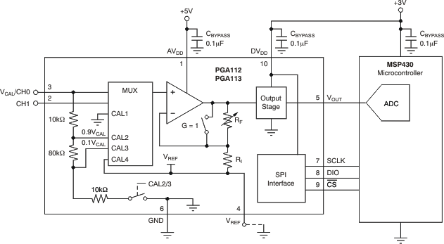
The PGA112 and PGA113 devices (binary and scope gains) offer two analog inputs, a three-pin SPI interface, and software shutdown in a 10-pin, VSSOP package. The PGA116 and PGA117 (binary and scope gains) offer 10 analog inputs, a SPI interface with daisy-chain capability, and hardware and software shutdown in a 20-pin TSSOP package.
All versions provide internal calibration channels for system-level calibration. The channels are tied to GND, 0.9 VCAL, 0.1 VCAL, and VREF, respectively. VCAL, an external voltage connected to Channel 0, is used as the system calibration reference. Binary gains are: 1, 2, 4, 8, 16, 32, 64, and 128; scope gains are: 1, 2, 5, 10, 20, 50, 100, and 200.
Device Information(1)
| PART NUMBER | PACKAGE | BODY SIZE (NOM) |
|---|---|---|
| PGA112, PGA113 | VSSOP (10) | 3.00 mm × 3.00 mm |
| PGA116, PGA117 | TSSOP (20) | 6.50 mm × 4.40 mm |
- For all available packages, see the orderable addendum at the end of the data sheet.
Simplified Schematic
