-
PGA900 Programmable Resistive Sensing Conditioner With Digital and Analog Outputs
Package Options
Mechanical Data (Package|Pins)
Thermal pad, mechanical data (Package|Pins)
Orderable Information
PGA900 Programmable Resistive Sensing Conditioner With Digital and Analog Outputs
1 Features
- High accuracy, low noise, low power, small size resistive sensing signal conditioner
- User-programmable temperature and nonlinearity compensation
- On-chip ARM®Cortex® M0 microprocessor allows users to develop and implement calibration software
- One-wire interface enables the communication through power supply pin without using additional lines
- On-chip power management accepts wide power supply voltage from 3.3 V to 30 V
- Operating temperature range: –40°C to +150°C
- Memory:
- 8-kB software memory
- 128 bytes EEPROM
- 1-kB data SRAM
- Accommodates sensor sensitivities from 1 mV/V to 135 mV/V
- Two individual analog-front end (AFE) chains, each including:
- Low-noise programmable gain amplifier
- 24-bit sigma-delta analog-to-digital converter
- Built-in internal temperature sensor with option to use external temperature sensor
- 14-bit DAC with programmable gain amplifier
- Output options:
- Ratiometric and absolute voltage output
- 4- to 20-mA current loop interface
- One-wire interface (OWI) over power line
- PWM output
- Serial peripheral interface (SPI)
- Inter-integrated circuit (I2C)
- Depletion MOSFET gate driver
- Diagnostic functions
2 Applications
- Pressure sensor transmitters and transducers
- Liquid level meters and flow meters
- Weight scales, load meters, and strain gauges
- Thermocouples, thermistors, and 2-wire resistance thermometers (RTD)
- Resistive field transmitters
3 Description
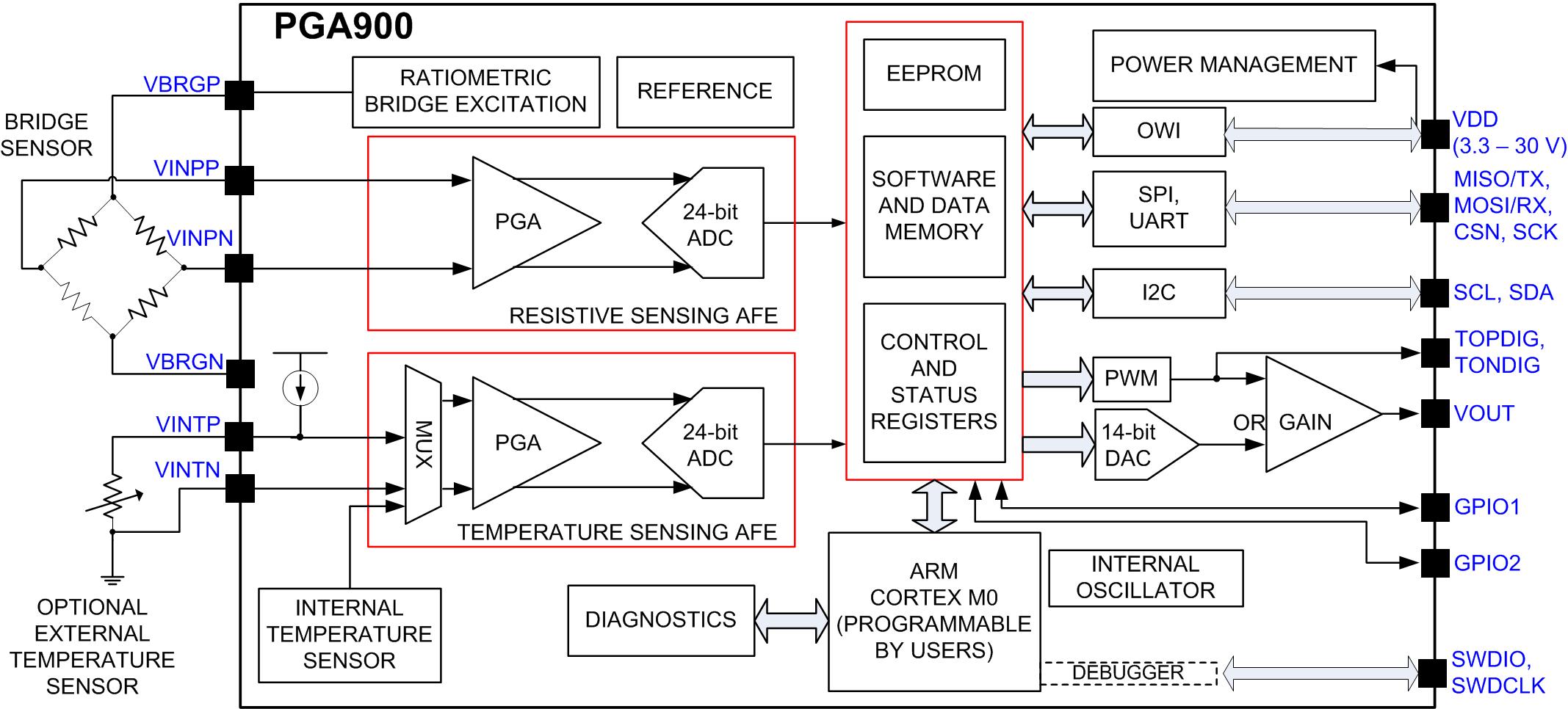
The PGA900 is a signal conditioner for resistive sensing applications. It can accommodate various sensing element types. The PGA900 conditions its input signals by amplification and digitization through two analog front end channels. With the user programmed software in the on-chip ARM Cortex M0 processor, the PGA900 can perform linearization, temperature compensation, and other user defined compensation algorithms. The conditioned signal can be output as ratiometric voltage, absolute voltage, 4- to 20-mA current loop or PWM. The data and configuration registers can also be accessed through SPI, I2C, UART, and two GPIO ports. In addition, the unique OWI allows communication and configuration through the power supply pin without using additional lines. The PGA900 operating voltage is from 3.3 V to 30 V and it can operate in temperatures from –40°C to +150°C.
Device Information(1)
| NUMBER | PACKAGE | BODY SIZE (NOM) |
|---|---|---|
| PGA900 | VQFN (36) | 6.00 mm × 6.00 mm |
| DSBGA (36) | 3.66 mm × 3.66 mm |
- For all available packages, see the orderable addendum at the end of the data sheet.
Device Images
PGA900 Simplified Block Diagram
