SBAS798 September 2017 REF2125
PRODUCTION DATA.
- 1 Features
- 2 Applications
- 3 Description
- 4 Revision History
- 5 Pin Configuration and Functions
- 6 Specifications
- 7 Parameter Measurement Information
- 8 Detailed Description
- 9 Applications and Implementation
- 10Power-Supply Recommendations
- 11Layout
- 12Device and Documentation Support
- 13Mechanical, Packaging, and Orderable Information
Package Options
Mechanical Data (Package|Pins)
- DBV|5
Thermal pad, mechanical data (Package|Pins)
Orderable Information
1 Features
- Initial Accuracy: ±0.05% (maximum)
- Temperature Coefficient : 6 ppm/°C (maximum)
- Operating Temperature Range: −40°C to +125°C
- Output Current: ±10 mA
- Low Quiescent Current: 95 μA (maximum)
- Wide Input Voltage: 12 V
- Output 1/f Noise (0.1 Hz to 10 Hz): 5 µVPP/V
- Excellent Long-Term Stability 30 ppm/1000 hrs
- Small Footprint 5-Pin SOT-23 Package
2 Applications
- Precision Data Acquisition Systems
- Power Monitoring
- PLC Analog I/O Modules
- Industrial Instrumentation
- Field Transmitters
- Test Equipment
- 4 - 20mA Loop sensors
- LCR Meters
3 Description
The REF2125 device is a low temperature drift
(6 ppm/°C), low-power, high-precision CMOS voltage reference, featuring ±0.05% initial accuracy, low operating current with power consumption less than 95 μA. This device also offers very low output noise of 5 μVp-p /V, which enables its ability to maintain high signal integrity with high-resolution data converters and noise critical systems.
Stability and system reliability are further improved by the low output-voltage hysteresis of the device and low long-term output voltage drift. Furthermore, the small size and low operating current of the devices (95 μA) make them ideal for portable and battery-powered applications.
REF2125 is specified for the wide temperature range of −40°C to +125°C. Contact the TI sales representative for additional voltage options.
Device Information(1)
| PART NAME | PACKAGE | BODY SIZE (NOM) |
|---|---|---|
| REF2125 | SOT-23 (5) | 2.90 mm × 1.60 mm |
- For all available packages, see the orderable addendum at the end of the datasheet.
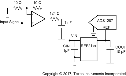
Simplified Schematic
