6 Specifications
6.1 Absolute Maximum Ratings
over operating free-air temperature range (unless otherwise noted)(1)
|
MIN |
MAX |
UNIT |
| Input voltage |
VIN |
|
18 |
V |
| Output short-circuit |
|
30 |
mA |
| Operating temperature |
–55 |
125 |
°C |
| Junction temperature, TJ |
|
150 |
°C |
| Storage temperature, Tstg |
–65 |
150 |
°C |
(1) Stresses above these ratings may cause permanent damage. Exposure to absolute maximum conditions for extended periods may degrade device reliability. These are stress ratings only, and functional operation of the device at these or any other conditions beyond those specified is not implied.
6.2 ESD Ratings
|
VALUE |
UNIT |
| V(ESD) |
Electrostatic discharge |
Human body model (HBM), per ANSI/ESDA/JEDEC JS-001(1) |
±3000 |
V |
| Charged-device model (CDM), per JEDEC specification JESD22-C101(2) |
±1000 |
(1) JEDEC document JEP155 states that 500-V HBM allows safe manufacturing with a standard ESD control process.
(2) JEDEC document JEP157 states that 250-V CDM allows safe manufacturing with a standard ESD control process.
6.3 Recommended Operating Conditions
over operating free-air temperature range (unless otherwise noted)
|
MIN |
MAX |
UNIT |
| VIN |
VOUT + 0.2 V |
18 |
V |
| IOUT |
–10 |
10 |
mA |
6.4 Thermal Information
| THERMAL METRIC(1) |
REF502x-EP |
UNIT |
| D (SOIC) |
| 8 PINS |
| RθJA |
Junction-to-ambient thermal resistance |
97.1 |
°C/W |
| RθJC(top) |
Junction-to-case (top) thermal resistance |
42.2 |
°C/W |
| RθJB |
Junction-to-board thermal resistance |
34.6 |
°C/W |
(1) For more information about traditional and new thermal metrics, see the
Semiconductor and IC Package Thermal Metrics application report,
SPRA953.
6.5 Electrical Characteristics: Per Device
At TA = 25°C, ILOAD = 0, CL = 1 μF, and VIN = (VOUT + 0.2 V) to 18 V, unless otherwise noted.
| PARAMETER |
TEST CONDITIONS |
TA = 25°C |
TA = –55°C to 125°C |
UNIT |
| MIN |
TYP |
MAX |
MIN |
TYP |
MAX |
| REF5020 (VOUT = 2.048V)(1) |
| OUTPUT VOLTAGE |
| Output Voltage |
VOUT |
2.7 V < VIN < 18 V |
|
2.048 |
|
|
|
|
V |
| Initial Accuracy |
|
|
–0.05% |
|
0.05% |
|
|
|
|
|
Over Temperature |
|
|
|
|
–0.08% |
|
0.08% |
|
| NOISE |
| Output Voltage Noise |
f = 0.1 Hz to 10 Hz |
|
6 |
|
|
|
|
μVPP |
| REF5025 (VOUT = 2.5 V) |
| OUTPUT VOLTAGE |
| Output Voltage |
VOUT |
|
|
2.5 |
|
|
|
|
V |
| Initial Accuracy |
|
–0.05% |
|
0.05% |
|
|
|
|
| NOISE |
| Output Voltage Noise |
f = 0.1 Hz to 10 Hz |
|
7.5 |
|
|
|
|
μVPP |
| REF5040 (VOUT = 4.096V) |
| OUTPUT VOLTAGE |
|
|
|
|
|
|
|
|
| Output Voltage |
VOUT |
|
|
4.096 |
|
|
|
|
V |
| Initial Accuracy |
|
–0.05% |
|
0.05% |
|
|
|
|
|
Over Temperature |
|
|
|
|
|
–0.08% |
|
0.08% |
|
| NOISE |
| Output Voltage Noise |
f = 0.1 Hz to 10 Hz |
|
12 |
|
|
|
|
μVPP |
| REF5050 (VOUT = 5 V) |
| OUTPUT VOLTAGE |
| Output Voltage |
VOUT |
|
|
5 |
|
|
|
|
V |
| Initial Accuracy |
|
–0.05% |
|
0.05% |
|
|
|
|
|
Over Temperature |
|
|
|
|
|
–0.08% |
|
0.08% |
|
| NOISE |
| Output Voltage Noise |
f = 0.1 Hz to 10 Hz |
|
15 |
|
|
|
|
μVPP |
(1) For VOUT ≤ 2.5 V, the minimum supply voltage is 2.7 V.
6.6 Electrical Characteristics: All Devices
At TA = 25°C, ILOAD = 0, CL = 1 μF, and VIN = (VOUT + 0.2 V) to 18 V, unless otherwise noted.
| PARAMETER |
TEST CONDITIONS |
TA = 25°C |
TA = –55°C to 125°C |
UNIT |
| MIN |
TYP |
MAX |
MIN |
TYP |
MAX |
| OUTPUT VOLTAGE TEMPERATURE DRIFT |
| Output Voltage Temperature Drift |
dVOUT/dT |
|
|
|
|
|
|
|
|
|
REF5025 |
|
|
|
|
|
4 |
6.5 |
ppm/°C |
|
REF5050 |
|
|
|
|
|
4 |
6.5 |
ppm/°C |
|
All other devices |
|
|
|
|
|
3 |
5 |
ppm/°C |
| LINE REGULATION |
| Line Regulation |
dVOUT/dVIN |
|
|
|
|
|
|
|
|
|
REF5020(1) |
VIN = 2.7 V to 18V |
|
0.1 |
1 |
|
|
|
ppm/V |
|
All other devices |
VIN = VOUT + 0.2 V |
|
0.1 |
1 |
|
|
|
ppm/V |
|
Over Temperature |
|
|
|
|
|
1 |
3 |
ppm/V |
| LOAD REGULATION |
| Load Regulation |
dVOUT/dILOAD |
|
|
|
|
|
|
|
|
|
REF5020 |
–10 mA < ILOAD < +10 mA, VIN = 3 V |
|
20 |
30 |
|
|
|
ppm/mA |
|
All other devices |
–10 mA < ILOAD < +10 mA, VIN = VOUT + 0.75 V |
|
20 |
30 |
|
|
|
ppm/mA |
|
Over Temperature |
|
|
|
|
|
|
60 |
ppm/mA |
| SHORT-CIRCUIT CURRENT |
| Short-Circuit Current |
ISC |
VOUT = 0 |
|
25 |
|
|
|
|
mA |
| TEMP PIN |
| Voltage Output |
At TA = 25°C |
|
575 |
|
|
|
|
mV |
| Temperature Sensitivity |
|
|
|
|
|
2.64 |
|
mV/°C |
| TURNON SETTLING TIME |
| Turnon Settling Time |
To 0.1% with CL = 1 μF |
|
200 |
|
|
|
|
μs |
| POWER SUPPLY |
| Supply Voltage |
VIN |
See Note (1) |
VOUT + 0.2(1) |
|
18 |
|
|
|
V |
| Quiescent Current |
|
|
0.8 |
1 |
|
|
|
mA |
| Over Temperature |
|
|
|
|
|
|
1.25 |
mA |
| TEMPERATURE RANGE |
| Specified Range |
|
–55 |
|
125 |
|
|
|
°C |
| Operating Range |
|
–55 |
|
125 |
|
|
|
°C |
| Thermal Resistance |
θJA |
|
|
150 |
|
|
|
|
°C/W |
(1) For VOUT ≤ 2.5 V, the minimal supply voltage is 2.7 V.
6.7 Typical Characteristics
At TA = 25°C, ILOAD = 0, and VIN = VOUT + 0.2 V, unless otherwise noted. For VOUT ≤ 2.5 V, the minimum supply voltage is 2.7 V.
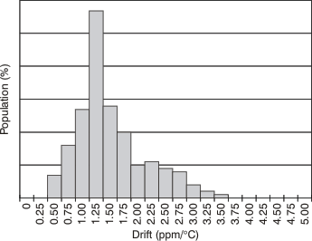
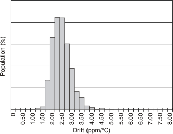
 Figure 1. Temperature Drift
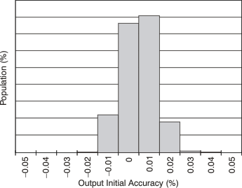
 Figure 3. Output Voltage Initial Accuracy
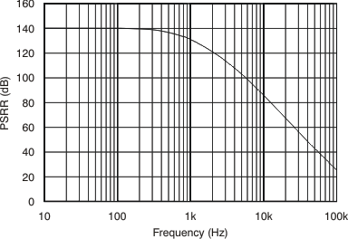
 Figure 5. Power-Supply Rejection Ratio vs Frequency
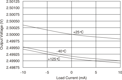
 Figure 7. REF5025 Output Voltage vs Load Current
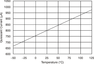
 Figure 9. Quiescent Current vs Temperature
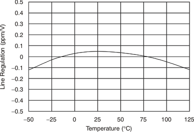
 Figure 11. Line Regulation vs Temperature
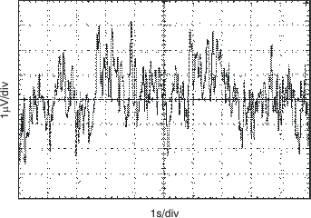
 Figure 13. NOISE
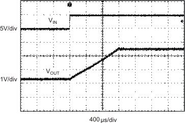
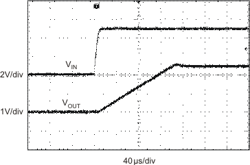
 Figure 15. Start-up
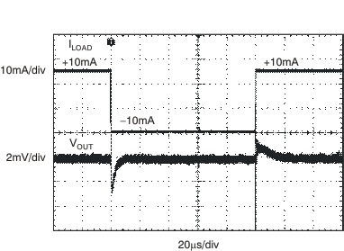
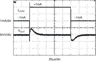
 Figure 17. Load Transient
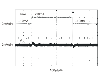
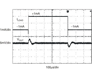
 Figure 19. Load Transient
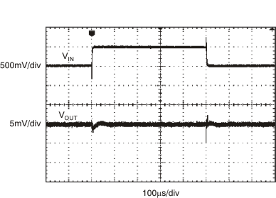
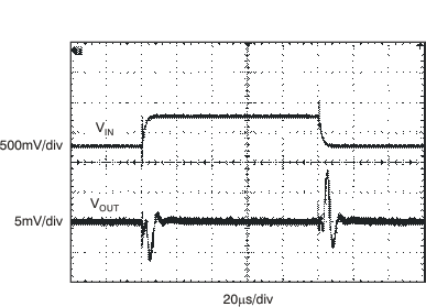
 Figure 21. Line Transient
 Figure 2. Temperature Drift
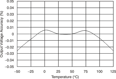
 Figure 4. Output Voltage Accuracy vs Temperature
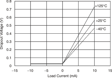
 Figure 6. Dropout Voltage vs Load Current
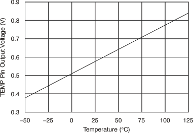
 Figure 8. Temp Pin Output vs Voltage Temperature
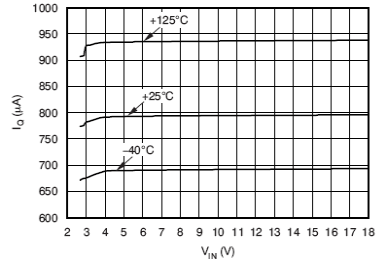
 Figure 10. Quiescent Current vs Input Voltage
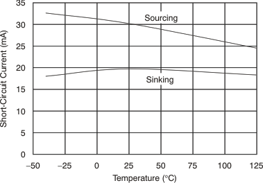
 Figure 12. Short-Circuit Current vs Temperature
 Figure 14. Start-up
 Figure 16. Load Transient
 Figure 18. Load Transient
 Figure 20. Line Transient
