SBOS410M June 2007 – December 2024 REF5010 , REF5020 , REF5025 , REF5030 , REF5040 , REF5045 , REF5050
PRODUCTION DATA
- 1
- 1 Features
- 2 Applications
- 3 Description
- 4 Device Comparison Table
- 5 Pin Configuration and Functions
- 6 Specifications
- 7 Parameter Measurement Information
- 8 Detailed Description
- 9 Applications and Implementation
- 10Power Supply Recommendations
- 11Layout
- 12Device and Documentation Support
- 13Revision History
- 14Mechanical, Packaging, and Orderable Information
Package Options
Mechanical Data (Package|Pins)
Thermal pad, mechanical data (Package|Pins)
Orderable Information
3 Description
The REF50xx is a family of low-noise, low-drift, very high precision voltage references. These references are capable of both sinking and sourcing current, and have excellent line and load regulation.
Excellent temperature drift (2.5ppm/°C) and high accuracy (0.025%) are achieved using proprietary design techniques. These features, combined with very low flicker noise (0.5μVPP/V), make the REF50xx family an excellent choice for use in high-precision data acquisition systems. REF50 family is available in enhanced grade (REF50xxEI), high grade (REF50xxI) and standard grade (REF50xxAI). The reference voltages are offered in 8-pin SOIC and VSSOP packages and are specified from –40°C to 125°C.
The REF50xxEI supports wide supply voltage rating of 42V with ultra-low IQ of 340μA. The wide supply range allows for direct connection to the battery or field supply. This also protects the device in case of power supply IC failure.
| PART NUMBER | PACKAGE (1) | BODY SIZE (NOM) (2) |
|---|---|---|
| REF50xxI , REF50xxAI | SOIC (8) | 4.90mm × 3.91mm |
| VSSOP (8) | 3.00mm × 3.00mm | |
| REF50xxEI | SOIC (8) | 4.90mm × 3.91mm |
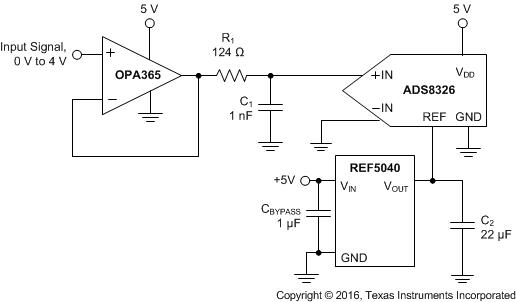
 Simplified Schematic