SBOS410L June   2007  – October 2024 REF5010 , REF5020 , REF5025 , REF5030 , REF5040 , REF5045 , REF5050

PRODUCTION DATA  

  1.   1
  2. Features
  3. Applications
  4. Description
  5. Device Comparison Table
  6. Pin Configuration and Functions
  7. Specifications
    1. 6.1 Absolute Maximum Ratings
    2. 6.2 ESD Ratings
    3. 6.3 Recommended Operating Conditions
    4. 6.4 Thermal Information
    5. 6.5 Electrical Characteristics REF50
    6. 6.6 Electrical Characteristics REF50EI
    7. 6.7 Typical Characteristics: REF50xxI, REF50xxAI
    8. 6.8 Typical Characteristics: REF50xxEI
  8. Parameter Measurement Information
    1. 7.1 Solder Heat Shift
  9. Detailed Description
    1. 8.1 Overview
    2. 8.2 Functional Block Diagram
    3. 8.3 Feature Description
      1. 8.3.1 Temperature Monitoring
      2. 8.3.2 Temperature Drift
      3. 8.3.3 Thermal Hysteresis
      4. 8.3.4 Noise Performance
      5. 8.3.5 Long-Term Stability
      6. 8.3.6 Output Adjustment Using the TRIM/NR Pin
    4. 8.4 Device Functional Modes
      1. 8.4.1 Basic Connections
      2. 8.4.2 Supply Voltage
      3. 8.4.3 Negative Reference Voltage
  10. Applications and Implementation
    1. 9.1 Application Information
    2. 9.2 Typical Applications
      1. 9.2.1 16-Bit, 250-KSPS Data Acquisition System
        1. 9.2.1.1 Design Requirements
        2. 9.2.1.2 Detailed Design Procedure
        3. 9.2.1.3 Application Curve
  11. 10Power Supply Recommendations
  12. 11Layout
    1. 11.1 Layout Guidelines
    2. 11.2 Layout Example
    3. 11.3 Power Dissipation
  13. 12Device and Documentation Support
    1. 12.1 Documentation Support
      1. 12.1.1 Related Documentation
    2. 12.2 Receiving Notification of Documentation Updates
    3. 12.3 Support Resources
    4. 12.4 Trademarks
    5. 12.5 Glossary
  14. 13Revision History
  15. 14Mechanical, Packaging, and Orderable Information

Package Options

Mechanical Data (Package|Pins)
Thermal pad, mechanical data (Package|Pins)
Orderable Information

Noise Performance

Typical 0.1Hz to 10Hz voltage noise for each member of the REF50xx family is specified in the Electrical Characteristics table. The noise voltage increases with output voltage and operating temperature. Additional filtering can be used to improve output noise levels, although take care to make sure the output impedance does not degrade performance.

For additional information about how to minimize noise and maximize performance in mixed-signal applications such as data converters, refer to the How a Voltage Reference Affects ADC Performance Part 1, How a Voltage Reference Affects ADC Performance Part 2, and How a Voltage Reference Affects ADC Performance Part 3 analog design journals.
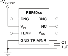
REF5010 REF5020 REF5025 REF5030 REF5040 REF5045 REF5050 Noise
                    Reduction Using the TRIM/NR Pin Figure 8-4 Noise Reduction Using the TRIM/NR Pin