SBOS410L June   2007  – October 2024 REF5010 , REF5020 , REF5025 , REF5030 , REF5040 , REF5045 , REF5050

PRODUCTION DATA  

  1.   1
  2. Features
  3. Applications
  4. Description
  5. Device Comparison Table
  6. Pin Configuration and Functions
  7. Specifications
    1. 6.1 Absolute Maximum Ratings
    2. 6.2 ESD Ratings
    3. 6.3 Recommended Operating Conditions
    4. 6.4 Thermal Information
    5. 6.5 Electrical Characteristics REF50
    6. 6.6 Electrical Characteristics REF50EI
    7. 6.7 Typical Characteristics: REF50xxI, REF50xxAI
    8. 6.8 Typical Characteristics: REF50xxEI
  8. Parameter Measurement Information
    1. 7.1 Solder Heat Shift
  9. Detailed Description
    1. 8.1 Overview
    2. 8.2 Functional Block Diagram
    3. 8.3 Feature Description
      1. 8.3.1 Temperature Monitoring
      2. 8.3.2 Temperature Drift
      3. 8.3.3 Thermal Hysteresis
      4. 8.3.4 Noise Performance
      5. 8.3.5 Long-Term Stability
      6. 8.3.6 Output Adjustment Using the TRIM/NR Pin
    4. 8.4 Device Functional Modes
      1. 8.4.1 Basic Connections
      2. 8.4.2 Supply Voltage
      3. 8.4.3 Negative Reference Voltage
  10. Applications and Implementation
    1. 9.1 Application Information
    2. 9.2 Typical Applications
      1. 9.2.1 16-Bit, 250-KSPS Data Acquisition System
        1. 9.2.1.1 Design Requirements
        2. 9.2.1.2 Detailed Design Procedure
        3. 9.2.1.3 Application Curve
  11. 10Power Supply Recommendations
  12. 11Layout
    1. 11.1 Layout Guidelines
    2. 11.2 Layout Example
    3. 11.3 Power Dissipation
  13. 12Device and Documentation Support
    1. 12.1 Documentation Support
      1. 12.1.1 Related Documentation
    2. 12.2 Receiving Notification of Documentation Updates
    3. 12.3 Support Resources
    4. 12.4 Trademarks
    5. 12.5 Glossary
  14. 13Revision History
  15. 14Mechanical, Packaging, and Orderable Information

Package Options

Mechanical Data (Package|Pins)
Thermal pad, mechanical data (Package|Pins)
Orderable Information

Negative Reference Voltage

For applications requiring a negative and positive reference voltage, the REF50xx and OPA735 can be used to provide a dual-supply reference from a 5V supply. Figure 8-7 shows the REF5025 used to provide a 2.5V supply reference voltage. The low-drift performance of the REF50xx complements the low offset voltage and zero drift of the OPA735 to provide an accurate solution for split-supply applications. Take care to match the temperature coefficients of R1 and R2.
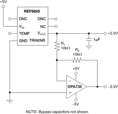
REF5010 REF5020 REF5025 REF5030 REF5040 REF5045 REF5050 The REF5025 and OPA735 Create Positive and Negative Reference VoltagesFigure 8-7 The REF5025 and OPA735 Create Positive and Negative Reference Voltages