SBOS410L June 2007 – October 2024 REF5010 , REF5020 , REF5025 , REF5030 , REF5040 , REF5045 , REF5050
PRODUCTION DATA
- 1
- 1 Features
- 2 Applications
- 3 Description
- 4 Device Comparison Table
- 5 Pin Configuration and Functions
- 6 Specifications
- 7 Parameter Measurement Information
- 8 Detailed Description
- 9 Applications and Implementation
- 10Power Supply Recommendations
- 11Layout
- 12Device and Documentation Support
- 13Revision History
- 14Mechanical, Packaging, and Orderable Information
Package Options
Mechanical Data (Package|Pins)
Thermal pad, mechanical data (Package|Pins)
Orderable Information
8.3.1 Temperature Monitoring
The temperature output terminal (TEMP, pin 3) provides a temperature-dependent voltage output with approximately 60kΩ source impedance. As illustrated in Figure 6-8, the output voltage follows the nominal relationship:
This pin indicates general chip temperature, accurate to approximately ±15°C. Although not generally suitable for accurate temperature measurements, this pin can be used to indicate temperature changes or for temperature compensation of analog circuitry. A temperature change of 30°C corresponds to an approximate 79mV change in voltage at the TEMP pin.
The TEMP pin has high-output impedance (see Section 8.2). Loading this pin with a low-impedance circuit induces a measurement error; however, this pin does not have any effect on VOUT accuracy.
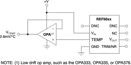
To avoid errors caused by low-impedance loading, buffer the TEMP pin output with a suitable low-temperature drift op amp, such as the OPA333, OPA335, or OPA376, as shown in Figure 8-3.
 Figure 8-3 Buffering the TEMP Pin Output