SBOS410L June   2007  – October 2024 REF5010 , REF5020 , REF5025 , REF5030 , REF5040 , REF5045 , REF5050

PRODUCTION DATA  

  1.   1
  2. Features
  3. Applications
  4. Description
  5. Device Comparison Table
  6. Pin Configuration and Functions
  7. Specifications
    1. 6.1 Absolute Maximum Ratings
    2. 6.2 ESD Ratings
    3. 6.3 Recommended Operating Conditions
    4. 6.4 Thermal Information
    5. 6.5 Electrical Characteristics REF50
    6. 6.6 Electrical Characteristics REF50EI
    7. 6.7 Typical Characteristics: REF50xxI, REF50xxAI
    8. 6.8 Typical Characteristics: REF50xxEI
  8. Parameter Measurement Information
    1. 7.1 Solder Heat Shift
  9. Detailed Description
    1. 8.1 Overview
    2. 8.2 Functional Block Diagram
    3. 8.3 Feature Description
      1. 8.3.1 Temperature Monitoring
      2. 8.3.2 Temperature Drift
      3. 8.3.3 Thermal Hysteresis
      4. 8.3.4 Noise Performance
      5. 8.3.5 Long-Term Stability
      6. 8.3.6 Output Adjustment Using the TRIM/NR Pin
    4. 8.4 Device Functional Modes
      1. 8.4.1 Basic Connections
      2. 8.4.2 Supply Voltage
      3. 8.4.3 Negative Reference Voltage
  10. Applications and Implementation
    1. 9.1 Application Information
    2. 9.2 Typical Applications
      1. 9.2.1 16-Bit, 250-KSPS Data Acquisition System
        1. 9.2.1.1 Design Requirements
        2. 9.2.1.2 Detailed Design Procedure
        3. 9.2.1.3 Application Curve
  11. 10Power Supply Recommendations
  12. 11Layout
    1. 11.1 Layout Guidelines
    2. 11.2 Layout Example
    3. 11.3 Power Dissipation
  13. 12Device and Documentation Support
    1. 12.1 Documentation Support
      1. 12.1.1 Related Documentation
    2. 12.2 Receiving Notification of Documentation Updates
    3. 12.3 Support Resources
    4. 12.4 Trademarks
    5. 12.5 Glossary
  14. 13Revision History
  15. 14Mechanical, Packaging, and Orderable Information

Package Options

Mechanical Data (Package|Pins)
Thermal pad, mechanical data (Package|Pins)
Orderable Information

Basic Connections

Figure 8-6 shows the typical connections for the REF50xx. TI recommends a supply bypass capacitor ranging from 1μF to 10μF. A 1μF to 50μF output capacitor (CL) must be connected from VOUT to GND. The equivalent series resistance (ESR) value of CL must be less than or equal to 1.5Ω to make sure output stability. To minimize noise, the recommended ESR of CL is from 1Ω and 1.5Ω.
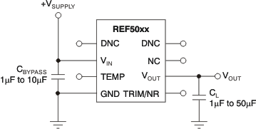
REF5010 REF5020 REF5025 REF5030 REF5040 REF5045 REF5050 Basic ConnectionsFigure 8-6 Basic Connections