SCLS970 November 2023 SN54SC4T125-SEP
PRODUCTION DATA
- 1
- 1 Features
- 2 Applications
- 3 Description
- 4 Pin Configuration and Functions
- 5 Specifications
- 6 Parameter Measurement Information
- 7 Detailed Description
- 8 Application and Implementation
- 9 Device and Documentation Support
- 10Revision History
- 11Mechanical, Packaging, and Orderable Information
Package Options
Mechanical Data (Package|Pins)
- PW|14
Thermal pad, mechanical data (Package|Pins)
Orderable Information
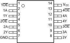
4 Pin Configuration and Functions
 Figure 4-1 PW Package,
14-Pin TSSOP
(Top View)
Table 4-1 Pin Functions
| PIN | TYPE(1) | DESCRIPTION | |
|---|---|---|---|
| NAME | NO. | ||
| 1OE | 1 | I | Channel 1, output enable, active low |
| 1A | 2 | I | Channel 1, input A |
| 1Y | 3 | O | Channel 1, output Y |
| 2OE | 4 | I | Channel 2, output enable, active low |
| 2A | 5 | I | Channel 2, input A |
| 2Y | 6 | O | Channel 2, output Y |
| GND | 7 | G | Ground |
| 3Y | 8 | O | Channel 3, output Y |
| 3A | 9 | I | Channel 3, input A |
| 3OE | 10 | I | Channel 3, output enable, active low |
| 4Y | 11 | O | Channel 4, output Y |
| 4A | 12 | I | Channel 4, input A |
| 4OE | 13 | I | Channel 4, output enable, active low |
| VCC | 14 | P | Positive supply |
(1) I = input, O = output, I/O = input or output, G =
ground, P = power.