SCLS970 November   2023 SN54SC4T125-SEP

PRODUCTION DATA  

  1.   1
  2. Features
  3. Applications
  4. Description
  5. Pin Configuration and Functions
  6. Specifications
    1. 5.1 Absolute Maximum Ratings
    2. 5.2 ESD Ratings
    3. 5.3 Recommended Operating Conditions
    4. 5.4 Thermal Information
    5. 5.5 Electrical Characteristics
    6. 5.6 Switching Characteristics
    7. 5.7 Noise Characteristics
    8. 5.8 Typical Characteristics
  7. Parameter Measurement Information
  8. Detailed Description
    1. 7.1 Overview
    2. 7.2 Functional Block Diagram
    3. 7.3 Feature Description
      1. 7.3.1 Balanced CMOS 3-State Outputs
      2. 7.3.2 Clamp Diode Structure
      3. 7.3.3 LVxT Enhanced Input Voltage
        1. 7.3.3.1 Down Translation
        2. 7.3.3.2 Up Translation
    4. 7.4 Device Functional Modes
  9. Application and Implementation
    1. 8.1 Application Information
    2. 8.2 Typical Application
      1. 8.2.1 Design Requirements
        1. 8.2.1.1 Power Considerations
        2. 8.2.1.2 Input Considerations
        3. 8.2.1.3 Output Considerations
      2. 8.2.2 Detailed Design Procedure
      3. 8.2.3 Application Curves
    3. 8.3 Power Supply Recommendations
    4. 8.4 Layout
      1. 8.4.1 Layout Guidelines
      2. 8.4.2 Layout Example
  10. Device and Documentation Support
    1. 9.1 Documentation Support
      1. 9.1.1 Related Documentation
    2. 9.2 Receiving Notification of Documentation Updates
    3. 9.3 Support Resources
    4. 9.4 Trademarks
    5. 9.5 Electrostatic Discharge Caution
    6. 9.6 Glossary
  11. 10Revision History
  12. 11Mechanical, Packaging, and Orderable Information

Package Options

Mechanical Data (Package|Pins)
Thermal pad, mechanical data (Package|Pins)
Orderable Information

Description

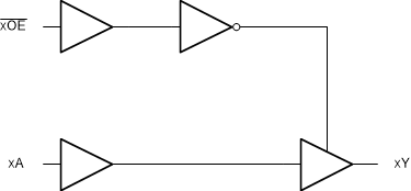
The SN54SC4T125-SEP contains four independent buffers with 3-state outputs and extended voltage operation to allow for level translation. Each buffer performs the Boolean function Y = A in positive logic. The outputs can be put into a high impedance (Hi-Z) state by applying a HIGH on the OE pin. The output level is referenced to the supply voltage (VCC) and supports 1.8-V, 2.5-V, 3.3-V, and 5-V CMOS levels.

The input is designed with a lower threshold circuit to support up translation for lower voltage CMOS inputs (for example, 1.2 V input to 1.8 V output or 1.8 V input to 3.3 V output). In addition, the 5-V tolerant input pins enable down translation (for example, 3.3 V to 2.5 V output).

Package Information
PART NUMBER PACKAGE(1) PACKAGE SIZE(2) BODY SIZE (NOM)(3)
SN54SC4T125-SEP PW (TSSOP, 14) 5 mm × 6.4 mm 5 mm × 4.4 mm
For more information, see Section 11.
The package size (length × width) is a nominal value and includes pins, where applicable.
The body size (length × width) is a nominal value and does not include pins.
GUID-9AB2696E-AB42-4889-90C9-96595DC92550-low.gif Simplified Logic Diagram (Positive Logic)