SLLS740C March 2007 – February 2024 SN65C1167E , SN65C1168E
PRODUCTION DATA
- 1
- 1 Features
- 2 Applications
- 3 Description
- 4 Pin Configuration and Functions
-
5 Specifications
- 5.1 Absolute Maximum Ratings
- 5.2 Driver Output and Receiver Input ESD Ratings
- 5.3 Recommended Operating Conditions
- 5.4 Thermal Information
- 5.5 Driver Section Electrical Characteristics
- 5.6 Receiver Section Electrical Characteristics
- 5.7 Driver Section Switching Characteristics
- 5.8 Receiver Section Switching Characteristics
- 6 Parameter Measurement Information
- 7 Detailed Description
- 8 Application and Implementation
- 9 Device and Documentation Support
- 10Revision History
- 11Mechanical, Packaging, and Orderable Information
Package Options
Mechanical Data (Package|Pins)
Thermal pad, mechanical data (Package|Pins)
- RGY|16
Orderable Information
8.1 Application Information
Figure 8-1 shows a typical RS-422 application. One transmitter is able to broadcast to multiple receiving nodes connected together over a shared differential bus. Twisted-pair cabling with a controlled differential impedance is used, and a termination resistance is placed at the farthest receive end of the cable in order to match the transmission line impedance and minimize signal reflections.
 Figure 8-1 Schematic of Inputs
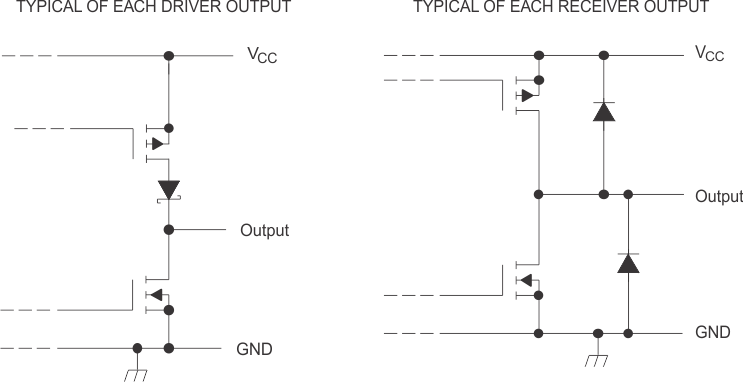
 Figure 8-2 Schematic of Outputs