SLLSES6C February 2016 – December 2021 SN65DP141
PRODUCTION DATA
- 1 Features
- 2 Applications
- 3 Description
- 4 Revision History
- 5 Pin Configuration and Functions
- 6 Specifications
- 7 Parameter Measurement Information
-
8 Detailed Description
- 8.1 Overview
- 8.2 Functional Block Diagram
- 8.3 Feature Description
- 8.4 Device Functional Modes
- 8.5
Register Maps
- 8.5.1 Register 0x00 (General Device Settings) (offset = 00000000) [reset = 00000000]
- 8.5.2 Register 0x01 (Channel Enable) (offset = 00000000) [reset = 00000000]
- 8.5.3 Register 0x02 (Channel 0 Control Settings) (offset = 00000000) [reset = 00000000]
- 8.5.4 Register 0x03 (Channel 0 Enable Settings) (offset = 00000000) [reset = 00000000]
- 8.5.5 Register 0x05 (Channel 1 Control Settings) (offset = 00000000) [reset = 00000000]
- 8.5.6 Register 0x06 (Channel 1 Enable Settings) (offset = 00000000) [reset = 00000000]
- 8.5.7 Register 0x08 (Channel 2 Control Settings) (offset = 00000000) [reset = 00000000]
- 8.5.8 Register 0x09 (Channel 2 Enable Settings) (offset = 00000000) [reset = 00000000]
- 8.5.9 Register 0x0B (Channel 3 Control Settings) (offset = 00000000) [reset = 00000000]
- 8.5.10 Register 0x0C (Channel 3 Control Settings) (offset = 00000000) [reset = 00000000]
- 9 Application and Implementation
- 10Power Supply Recommendations
- 11Layout
- 12Device and Documentation Support
- 13Mechanical, Packaging, and Orderable Information
Package Options
Mechanical Data (Package|Pins)
- RLJ|38
Thermal pad, mechanical data (Package|Pins)
Orderable Information
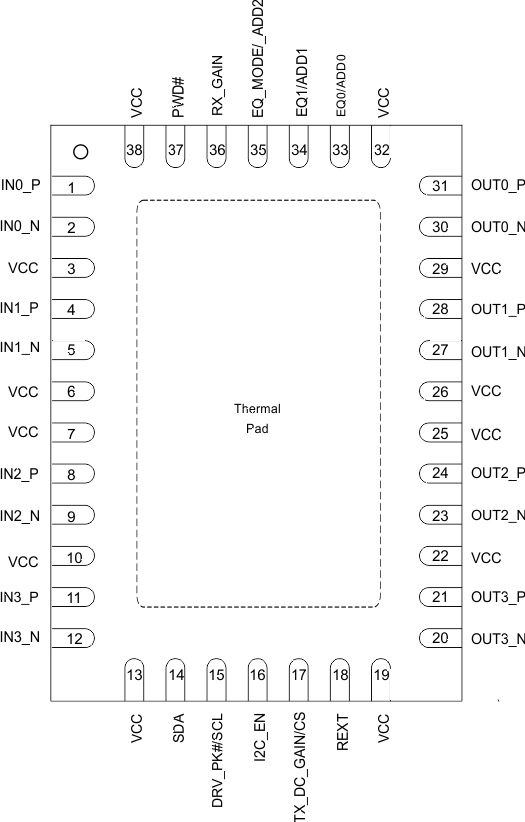
5 Pin Configuration and Functions

It is required for the thermal
pad to be soldered to ground for better thermal performance.
Figure 5-1 RLJ Package38 Pins (WQFN)Top ViewTable 5-1 Pin Functions
| PIN | TYPE(1) | DESCRIPTION | ||||||
|---|---|---|---|---|---|---|---|---|
| NAME | NO. | |||||||
| DIFFERENTIAL HIGH-SPEED I/O | ||||||||
| IN0_P | 1 | I | Differential input, lane 0 (with 50 Ω termination to input common mode) | |||||
| IN0_N | 2 | I | ||||||
| IN1_P | 4 | I | Differential input, lane 1 (with 50 Ω termination to input common mode) | |||||
| IN1_N | 5 | I | ||||||
| IN2_P | 8 | I | Differential input, lane 2 (with 50 Ω termination to input common mode) | |||||
| IN2_N | 9 | I | ||||||
| IN3_P | 11 | I | Differential input, lane 3 (with 50 Ω termination to input common mode) | |||||
| IN3_N | 12 | I | ||||||
| OUT0_P | 31 | O | Differential output, lane 0 | |||||
| OUT0_N | 30 | O | ||||||
| OUT1_P | 28 | O | Differential output, lane 1 | |||||
| OUT1_N | 27 | O | ||||||
| OUT2_P | 24 | O | Differential output, lane 2 | |||||
| OUT2_N | 23 | O | ||||||
| OUT3_P | 21 | O | Differential output, lane 3 | |||||
| OUT3_N | 20 | O | ||||||
| CONTROL SIGNALS | ||||||||
| DRV_PK#/SCL | 15 | I (with 200-kΩ internal pull-up) |
GPIO mode: HIGH: disable Driver peaking LOW: enables Driver 6-dB AC peaking |
I2C mode: I2C CLK. Connect a 10-kΩ pull-up resistor externally. |
||||
| EQ_MODE/ ADD2 | 35 | I (with 200-kΩ Internal pull-down, 2.5 V/3.3 V CMOS ) |
GPIO mode: HIGH: Trace mode LOW: Cable mode |
I2C mode: ADD2 along with pins ADD1 and ADD0 comprise the three bits of I2C slave address. ADD2:ADD1:ADD0:XXX |
||||
| EQ0/ADD0 | 33 | I (2.5 V/3.3 V CMOS - 3-state) |
GPIO mode: Working with RX_GAIN and EQ1 to determine the receiver DC and AC gain. |
I2C mode: ADD0 along with pins ADD1 and ADD2 comprise the three bits of I2C slave address. ADD2:ADD1:ADD0:XXX |
||||
| EQ1/ADD1 | 34 | I (2.5 V/3.3 V CMOS - 3-state) |
GPIO mode: Working with RX_GAIN and EQ0 to determine the receiver DC and AC gain. |
I2C mode: ADD1 along with pins ADD0 and ADD2 comprise the three bits of I2C slave address ADD2:ADD1:ADD0:XXX |
||||
| I2C_EN | 16 | I (with 200-kΩ internal pull-down) |
Configures the device operation for I2C
or GPIO mode: HIGH: enables I2C mode LOW: enables GPIO mode |
|||||
| PWD# | 37 | I (with 200-kΩ Internal pull-up, 2.5 V/3.3 V CMOS) |
HIGH: Normal Operation LOW: Power downs the device, inputs off and outputs disabled, resets I2C |
|||||
| REXT | 18 | I (analog) | External Bias Resistor: 1,200 Ω to GND | |||||
| RX_GAIN | 36 | I (2.5 V/3.3 V CMOS - 3-state) |
GPIO mode: Working with EQ0 and EQ1 to determine the receiver DC and AC gain. |
I2C mode: No action needed |
||||
| SDA | 14 | I/O (open drain) | GPIO mode: No action needed. |
I2C mode: I2C data. Connect a 10-kΩ pull-up resistor externally. |
||||
| TX_DC_GAIN/CS | 17 | I (with 200-kΩ Internal pull-down, 2.5 V/3.3 V CMOS) |
GPIO mode: HIGH: 6 dB DC gain for transmitter LOW: 0 dB DC gain for transmitter |
I2C mode: HIGH: acts as Chip Select LOW: disables I2C interface |
||||
| POWER SUPPLY | ||||||||
| GND Center Pad | Ground | The ground center pad is the metal contact at the bottom of the package. This pad must be connected to the GND plane. At least 15 PCB vias are recommended to minimize inductance and provide a solid ground. Refer to the package drawing (RLJ-package) for the via placement. | ||||||
| VCC | 3, 6, 7, 10, 13, 19, 22, 25, 26, 29, 32, 38 | Power | Power supply 2.5 V ±5%, 3.3 V ±5% | |||||
(1) I = input, O = output