SLLS753E February 2007 – September 2016 SN65HVD1040-Q1
PRODUCTION DATA.
- 1 Features
- 2 Applications
- 3 Description
- 4 Revision History
- 5 Description (continued)
- 6 Pin Configuration and Functions
-
7 Specifications
- 7.1 Absolute Maximum Ratings
- 7.2 ESD Ratings
- 7.3 Recommended Operating Conditions
- 7.4 Thermal Information
- 7.5 Electrical Characteristics: Supply Current
- 7.6 Electrical Characteristics: Driver
- 7.7 Electrical Characteristics: Receiver
- 7.8 Switching Characteristics: Device
- 7.9 Switching Characteristics: Driver
- 7.10 Switching Characteristics: Receiver
- 7.11 STB Pin Characteristics
- 7.12 SPLIT Pin Characteristics
- 7.13 Typical Characteristics
- 8 Parameter Measurement Information
- 9 Detailed Description
- 10Application and Implementation
- 11Power Supply Recommendations
- 12Layout
- 13Device and Documentation Support
- 14Mechanical, Packaging, and Orderable Information
Package Options
Refer to the PDF data sheet for device specific package drawings
Mechanical Data (Package|Pins)
- D|8
Thermal pad, mechanical data (Package|Pins)
Orderable Information
10 Application and Implementation
NOTE
Information in the following applications sections is not part of the TI component specification, and TI does not warrant its accuracy or completeness. TI’s customers are responsible for determining suitability of components for their purposes. Customers should validate and test their design implementation to confirm system functionality.
10.1 Application Information
10.1.1 CAN Nodes Using Common-Mode Chokes
The SN65HVD1040-Q1 has been EMC optimized to allow use in CAN systems without a common-mode choke. However, sometimes the CAN network and termination architecture may require their use. If a common-mode choke is used in a CAN node where bus line shorts to DC voltages may be possible, take care in the choice of common-mode choke (winding type, core type, and value) along with the termination and protection scheme of the node and bus. During CAN bus shorts to DC voltages the inductance of the common-mode choke may cause inductive flyback transients. Some combinations of common-mode chokes, bus termination, and shorting voltages can take the bus voltages outside the absolute maximum ratings of the device, possibly leading to damage.
10.2 Typical Application
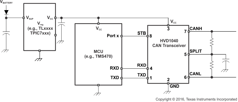 Figure 26. Typical Application Using Split Termination for Stabilization
10.2.1 Design Requirements
10.2.1.1 Bus Loading, Length, and Number of Nodes
The ISO 11898 Standard specifies up to 1 Mbps data rate, maximum bus length of 40 meters, maximum drop line (stub) length of 0.3 meters and a maximum of 30 nodes. However, with careful network design, the system may have longer cables, longer stub lengths, and many more nodes to a bus. Many CAN organizations and standards have scaled the use of CAN for applications outside the original ISO 11898 standard. They have made system level trade-offs for data rate, cable length, and parasitic loading of the bus. Examples of some of these specifications are SAE J1939, CANopen, DeviceNet, and NMEA2000.
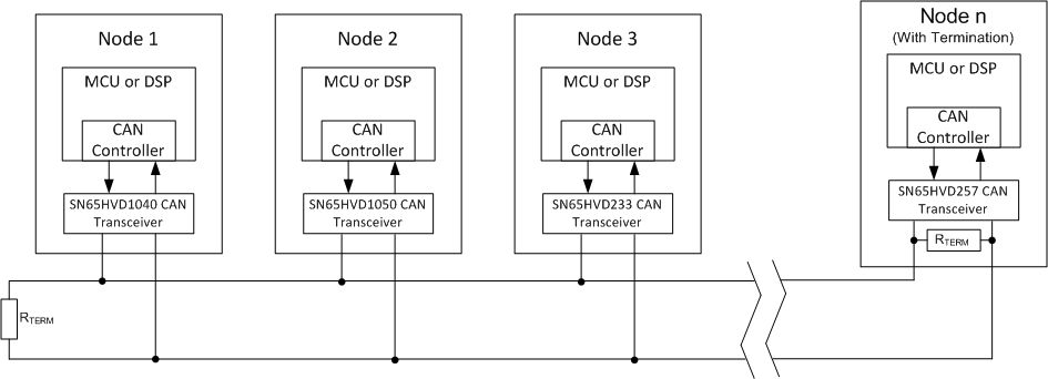 Figure 27. Typical CAN Bus
A high number of nodes requires a transceiver with high input impedance and wide common mode range such as the SN65HVD1040 CAN transceiver. ISO 11898-2 specifies the driver differential output with a 60-Ω load (two 120-Ω termination resistors in parallel) and the differential output must be greater than 1.5 V. The SN65HVD1040 device is specified to meet the 1.5-V requirement with a 60-Ω load, and additionally specified with a differential output voltage minimum of 1.2 V across a common-mode range of –2 V to 7 V through a 330-Ω coupling network. This network represents the bus loading of 90 SN65HVD1040 transceivers based on their minimum differential input resistance of 30 kΩ. Therefore, the SN65HVD1040 supports up to 90 transceivers on a single bus segment with margin to the 1.2-V minimum differential input voltage requirement at each node.
For CAN network design, margin must be given for signal loss across the system and cabling, parasitic loadings, network imbalances, ground offsets, and signal integrity, thus a practical maximum number of nodes may be lower. Bus length may also be extended beyond the original ISO 11898 standard of 40 meters by careful system design and data rate tradeoffs. For example, CANopen network design guidelines allow the network to be up to 1 km with changes in the termination resistance, cabling, less than 64 nodes and significantly lowered data rate.
This flexibility in CAN network design is one of the key strengths of the various extensions and additional standards that have been built on the original ISO 11898 CAN standard.
10.2.1.2 CAN Termination
The ISO 11898 standard specifies the interconnect to be a twisted pair cable (shielded or unshielded) with 120-Ω characteristic impedance (ZO ). Resistors equal to the characteristic impedance of the line must be used to terminate both ends of the cable to prevent signal reflections. Unterminated drop lines (stubs) connecting nodes to the bus must be kept as short as possible to minimize signal reflections. The termination may be on the cable or in a node, but if nodes may be removed from the bus the termination must be carefully placed so that it is not removed from the bus.
Termination is typically a 120-Ω resistor at each end of the bus. If filtering and stabilization of the common-mode voltage of the bus is desired, then split termination may be used (see Figure 28). Split termination uses two 60-Ω resistors with a capacitor in the middle of these resistors to ground. Split termination improves the electromagnetic emissions behavior of the network by eliminating fluctuations in the bus common mode voltages at the start and end of message transmissions.
Take care determining the power ratings of the termination resistors. A typical worst-case fault condition is if the system power supply and ground were shorted across the termination resistance which would result in much higher current through the termination resistance than the current limit of the CAN transceiver.
 Figure 28. CAN Termination
10.2.1.3 Loop Propagation Delay
Transceiver loop delay is a measure of the overall device propagation delay, consisting of the delay from the driver input (TXD pin) to the differential outputs (CANH and CANL pins), plus the delay from the receiver inputs (CANH and CANL) to its output (RXD pin). A typical loop delay for the SN65HVD1050 transceiver is displayed in Figure 32.
10.2.2 Detailed Design Procedure
10.2.2.1 CAN Basics
The basics of arbitration require that the receiver at the sending node designate the first bit as dominant or recessive after the initial wave of the first bit of a message travels to the most remote node on a network and back again. Typically, this sample is made at 75% of the bit width, and within this limitation, the maximum allowable signal distortion in a CAN network is determined by network electrical parameters.
Factors to be considered in network design include the approximately 5 ns/m propagation delay of typical twisted-pair bus cable; signal amplitude loss due to the loss mechanisms of the cable; and the number, length, and spacing of drop-lines (stubs) on a network. Under strict analysis, variations among the different oscillators in a system also must be accounted for with adjustments in signaling rate and stub and bus length. Table 5 lists the maximum signaling rates achieved with the SN65HVD1040 with several bus lengths of category 5, shielded twisted pair (CAT 5 STP) cable.
Table 5. Maximum Signaling Rates for Various Cable Lengths
| BUS LENGTH (m) | SIGNALING RATE (kbps) |
|---|---|
| 30 | 1000 |
| 100 | 500 |
| 250 | 250 |
| 500 | 125 |
| 1000 | 62.5 |
The Standard specifies the interconnect to be a single twisted-pair cable (shielded or unshielded) with 120-Ω characteristic impedance (ZO). Resistors equal to the characteristic impedance of the line terminate both ends of the cable to prevent signal reflections. Unterminated drop-lines connect nodes to the bus and must be kept as short as possible to minimize signal reflections.
Connectors, while not specified by the standard should have as little effect as possible on standard operating parameters such as capacitive loading. Although unshielded cable is used in many applications, data transmission circuits employing CAN transceivers are usually used in applications requiring a rugged interconnection with a wide common-mode voltage range. Therefore, shielded cable is recommended in these electronically harsh environments, and when coupled with the standard’s –2-V to 7-V common-mode range of tolerable ground noise, helps to ensure data integrity. The SN65HVD1040 enhances the standard’s insurance of data integrity with an extended –12 V to 12 V range of common-mode operation.
An eye pattern is a useful tool for measuring overall signal quality. As displayed in Figure 29, the differential signal changes logic states in two places on the display, producing an eye. Instead of viewing only one logic crossing on the scope, an entire bit of data is brought into view. The resulting eye pattern includes all of the effects of systemic and random distortion, and displays the time during which a signal may be considered valid.
The height of the eye above or below the receiver threshold voltage level at the sampling point is the noise margin of the system. Jitter is typically measured at the differential voltage zero-crossing during the logic state transition of a signal. Note that jitter present at the receiver threshold voltage level is considered by some to be a more effective representation of the jitter at the input of a receiver.
As the sum of skew and noise increases, the eye closes and data is corrupted. Closing the width decreases the time available for accurate sampling, and lowering the height enters the 900-mV or 500-mV threshold of a receiver.
Different sources induce noise onto a signal. The more obvious noise sources are the components of a transmission circuit themselves; the signal transmitter, traces and cables, connectors, and the receiver. Beyond that, there is a termination dependency, cross-talk from clock traces and other proximity effects, VCC and ground bounce, and electromagnetic interference from near-by electrical equipment.
The balanced receiver inputs of the SN65HVD1040 mitigate most all sources of signal corruption, and when used with a quality shielded twisted-pair cable, help insure data integrity.
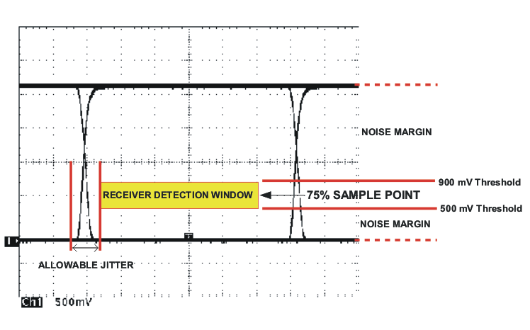 Figure 29. Typical CAN Differential Signal Eye-Pattern
10.2.2.1.1 Differential Signal
CAN is a differential bus where complementary signals are sent over two wires and the voltage difference between the two wires defines the logical state of the bus. The differential CAN receiver monitors this voltage difference and outputs the bus state with a single-ended logic level output signal.
The CAN driver creates the differential voltage between CANH and CANL in the dominant state. The dominant differential output of the SN65HVD1040 is greater than 1.5 V and less than 3 V across a 60-Ω load as defined by the ISO 11898 standard. Figure 30 shows CANH, CANL, and the differential dominant state level for the SN65HVD1040.
A CAN receiver is required to output a recessive state when less than 500 mV of differential voltage exists on the bus, and a dominant state when more than 900 mV of differential voltage exists on the bus. The CAN receiver must do this with common-mode input voltages from –2 V to 7 V.
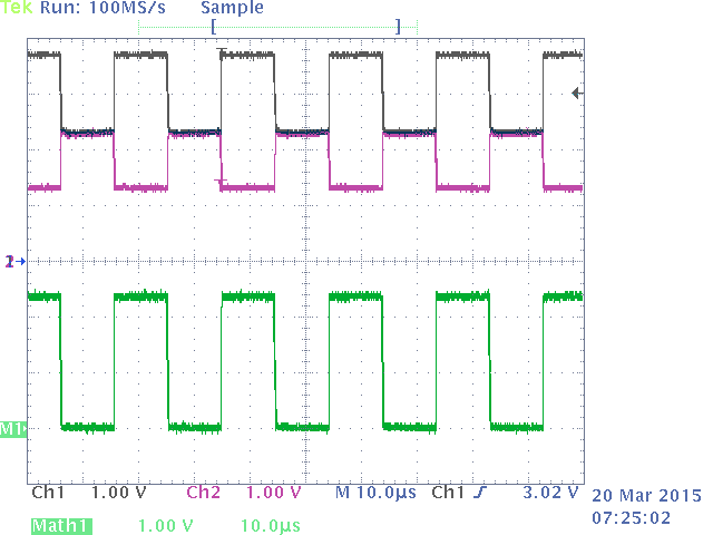 Figure 30. Differential Output Waveform
10.2.2.1.2 Common-Mode Signal
A common-mode or recessive signal is an average voltage of the two signal wires that the differential receiver rejects. The common-mode signal comes from the CAN driver, ground noise, and coupled bus noise. Because the bias voltage of the recessive state of the device is dependent on VCC , any noise present or variation of VCC has an effect on this bias voltage seen by the bus. The SN65HVD1040 CAN transceiver has the recessive bias voltage set to 0.5 × VCC to comply with the ISO 11898-2 CAN standard.
10.2.2.1.3 ESD Protection
A typical application that employees a CAN bus network may require some form of ESD, burst, and surge protection to shield the CAN transceiver against unwanted transients that can potential damage the transceiver. To help shield the SN65HVD1040 transceiver against these high energy transients, transient voltage suppressors can be implemented on the CAN differential bus terminals. These devices will help absorb the impact of a ESD, burst, or surge strike.
10.2.2.1.4 Transient Voltage Suppresser (TVS) Diodes
Transient voltage suppressors are the preferred protection components for a CAN bus due to their low capacitance, which allows them to be designed into every node of a multi-node network without requiring a reduction in data rate. With response times of a few picoseconds and power ratings of up to several kilowatts, TVS diodes present the most effective protection against ESD, burst, and surge transients.
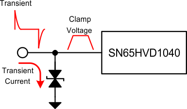 Figure 31. Transient
10.2.3 Application Curve
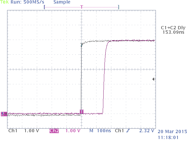 Figure 32. tloop Delay Waveform