SLLS994B February   2010  – July 2015 SN65HVDA1050A-Q1

PRODUCTION DATA.  

  1. Features
  2. Applications
  3. Description
  4. Revision History
  5. Pin Configuration and Functions
  6. Specifications
    1. 6.1 Absolute Maximum Ratings
    2. 6.2 ESD Ratings
    3. 6.3 Recommended Operating Conditions
    4. 6.4 Thermal Information
    5. 6.5 Electrical Characteristics
    6. 6.6 Power Dissipation Characteristics
    7. 6.7 Switching Characteristics
    8. 6.8 Typical Characteristics
  7. Parameter Measurement Information
  8. Detailed Description
    1. 8.1 Overview
    2. 8.2 Functional Block Diagram
    3. 8.3 Feature Description
      1. 8.3.1 Operating Modes
        1. 8.3.1.1 Normal Mode
        2. 8.3.1.2 Silent Mode
      2. 8.3.2 Protection Features
        1. 8.3.2.1 TXD Dominant State Timeout
        2. 8.3.2.2 Thermal Shutdown
        3. 8.3.2.3 Undervoltage Lockout and Unpowered Device
    4. 8.4 Device Functional Modes
  9. Application and Implementation
    1. 9.1 Application Information
      1. 9.1.1 Using the Device With 3.3-V Microcontrollers
      2. 9.1.2 Using SPLIT (VREF) With Split Termination
    2. 9.2 Typical Application
      1. 9.2.1 Design Requirements
        1. 9.2.1.1 Bus Loading, Length, and Number of Nodes
        2. 9.2.1.2 CAN Termination
        3. 9.2.1.3 Loop Propagation Delay
      2. 9.2.2 Detailed Design Procedure
        1. 9.2.2.1 ESD Protection
        2. 9.2.2.2 Transient Voltage Suppresser (TVS) Diodes
      3. 9.2.3 Application Curves
  10. 10Power Supply Recommendations
  11. 11Layout
    1. 11.1 Layout Guidelines
    2. 11.2 Layout Example
  12. 12Device and Documentation Support
    1. 12.1 Community Resources
    2. 12.2 Trademarks
    3. 12.3 Electrostatic Discharge Caution
    4. 12.4 Glossary
  13. 13Mechanical, Packaging, and Orderable Information

Package Options

Mechanical Data (Package|Pins)
Thermal pad, mechanical data (Package|Pins)
Orderable Information

5 Pin Configuration and Functions

D Package
8-Pin SOIC
Top View
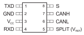
SN65HVDA1050A-Q1 pinout_lls994.gif

Pin Functions

PIN TYPE DESCRIPTION
NO. NAME
1 TXD I CAN transmit data input (low for dominant bus state, high for recessive bus state)
2 GND GND Ground connection
3 VCC Supply Transceiver 5-V supply voltage input
4 RXD O CAN receiver data output (low in dominant bus state, high in recessive bus state)
5 SPLIT (VREF) O Common-mode stabilization output for split termination
6 CANL I/O LOW-level CAN bus line
7 CANH I/O HIGH-level CAN bus line
8 S I Silent mode select pin (active-high)