SLLSEH7B December 2013 – June 2016 SN65LVPE512
PRODUCTION DATA.
- 1 Features
- 2 Applications
- 3 Description
- 4 Revision History
- 5 Pin Configuration and Functions
- 6 Specifications
- 7 Parameter Measurement Information
- 8 Detailed Description
- 9 Application and Implementation
- 10Power Supply Recommendations
- 11Layout
- 12Device and Documentation Support
- 13Mechanical, Packaging, and Orderable Information
Package Options
Mechanical Data (Package|Pins)
Thermal pad, mechanical data (Package|Pins)
- RGE|24
Orderable Information
7 Parameter Measurement Information
7.1 Typical Eye Diagram and Performance Curves
Measurement equipment details:
- Generator (source) LeCroy PERT3,
- Signal: 5 Gbps, 1000 mVp-p, 3.5-dB De-Emphasis
- TJ and DJ measurements based on CP0 (USB 3 compliance pattern) which is D0.0 or logical idle with SKP sequences removed
- RJ measurements based on CP1 or D10.2 symbol containing alternating 0s and 1s at Nyquist frequency
- Oscilloscope (Sink) LeCroy 25-GHz Real Time Oscilloscope
- LeCroy QualiPHY software used to measure jitter and collect compliance eye diagrams
Device Operating Conditions: VCC = 3.3 V, Temp = 25°C, EQx, DEx, OSx set to their default value when not mentioned
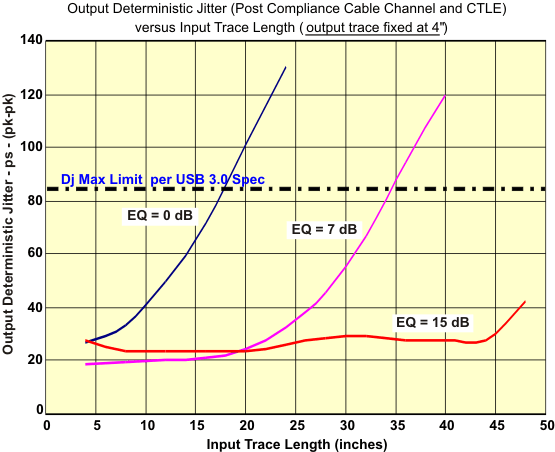
7.2 Plot 1 Fixed Output Trace +3-m USB 3 Cable With Variable Input Trace
 Figure 27. Parameter Measurement Set-Up
 Figure 28. Output DJ vs Input Trace Length With Different EQ Settings
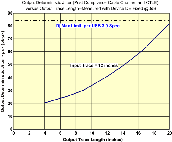
7.3 Plot 2 Fixed Input Trace With Variable Output Trace and +3-m USB 3.0 Cable
 Figure 29. Parameter Measurement Set-Up
 Figure 30. Output DJ
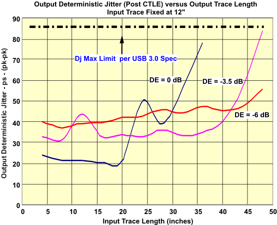
7.4 Plot 3 Fixed Input Trace With Variable Output Trace and (No Cable)
 Figure 31. Parameter Measurement Set-Up
 Figure 32. Output DJ vs Input Trace Length With Different EQ Settings