SLLSFG7B September 2020 – November 2022 SN65MLVD203B
PRODUCTION DATA
- 1 Features
- 2 Applications
- 3 Description
- 4 Revision History
- 5 Pin Configuration and Functions
-
6 Specifications
- 6.1 Absolute Maximum Ratings
- 6.2 ESD Ratings
- 6.3 Recommended Operating Conditions
- 6.4 Thermal Information
- 6.5 Electrical Characteristics
- 6.6 Electrical Characteristics – Driver
- 6.7 Electrical Characteristics – Receiver
- 6.8 Switching Characteristics – Driver
- 6.9 Switching Characteristics – Receiver
- 6.10 Typical Characteristics
- 7 Parameter Measurement Information
- 8 Detailed Description
-
9 Application and Implementation
- 9.1 Application Information
- 9.2
Typical Application
- 9.2.1 Multipoint Communications
- 9.2.2 Design Requirements
- 9.2.3
Detailed Design Procedure
- 9.2.3.1 Supply Voltage
- 9.2.3.2 Supply Bypass Capacitance
- 9.2.3.3 Driver Input Voltage
- 9.2.3.4 Driver Output Voltage
- 9.2.3.5 Termination Resistors
- 9.2.3.6 Receiver Input Signal
- 9.2.3.7 Receiver Input Threshold (Failsafe)
- 9.2.3.8 Receiver Output Signal
- 9.2.3.9 Interconnecting Media
- 9.2.3.10 PCB Transmission Lines
- 9.2.4 Application Curves
- 9.3 Power Supply Recommendations
- 9.4 Layout
- 10Device and Documentation Support
- 11Mechanical, Packaging, and Orderable Information
Package Options
Mechanical Data (Package|Pins)
- RUM|16
Thermal pad, mechanical data (Package|Pins)
- RUM|16
Orderable Information
9.2.3.7 Receiver Input Threshold (Failsafe)
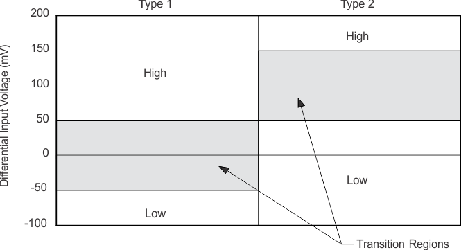
The MLVDS standard defines a Type-1 and Type-2 receiver. Type-1 receivers have their differential input voltage thresholds near zero volts. Type-2 receivers have their differential input voltage thresholds offset from 0 V to detect the absence of a voltage difference. The impact to receiver output by the offset input can be seen in Table 9-2 and Figure 9-3.
Table 9-2 Receiver Input Voltage Threshold Requirements
| RECEIVER TYPE | OUTPUT LOW | OUTPUT HIGH |
|---|---|---|
| Type 1 | –2.4 V ≤ VID ≤ –0.05 V | 0.05 V ≤ VID ≤ 2.4 V |
| Type 2 | –2.4 V ≤ VID ≤ 0.05 V | 0.15 V ≤ VID ≤ 2.4 V |
 Figure 9-3 Expanded Graph of Receiver Differential Input Voltage Showing Transition Region