SLLSFG7B September 2020 – November 2022 SN65MLVD203B
PRODUCTION DATA
- 1 Features
- 2 Applications
- 3 Description
- 4 Revision History
- 5 Pin Configuration and Functions
-
6 Specifications
- 6.1 Absolute Maximum Ratings
- 6.2 ESD Ratings
- 6.3 Recommended Operating Conditions
- 6.4 Thermal Information
- 6.5 Electrical Characteristics
- 6.6 Electrical Characteristics – Driver
- 6.7 Electrical Characteristics – Receiver
- 6.8 Switching Characteristics – Driver
- 6.9 Switching Characteristics – Receiver
- 6.10 Typical Characteristics
- 7 Parameter Measurement Information
- 8 Detailed Description
-
9 Application and Implementation
- 9.1 Application Information
- 9.2
Typical Application
- 9.2.1 Multipoint Communications
- 9.2.2 Design Requirements
- 9.2.3
Detailed Design Procedure
- 9.2.3.1 Supply Voltage
- 9.2.3.2 Supply Bypass Capacitance
- 9.2.3.3 Driver Input Voltage
- 9.2.3.4 Driver Output Voltage
- 9.2.3.5 Termination Resistors
- 9.2.3.6 Receiver Input Signal
- 9.2.3.7 Receiver Input Threshold (Failsafe)
- 9.2.3.8 Receiver Output Signal
- 9.2.3.9 Interconnecting Media
- 9.2.3.10 PCB Transmission Lines
- 9.2.4 Application Curves
- 9.3 Power Supply Recommendations
- 9.4 Layout
- 10Device and Documentation Support
- 11Mechanical, Packaging, and Orderable Information
Package Options
Mechanical Data (Package|Pins)
- RUM|16
Thermal pad, mechanical data (Package|Pins)
- RUM|16
Orderable Information
3 Description
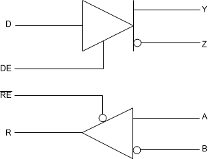
The SN65MLVD203B device is a multipoint low-voltage differential signaling (M-LVDS) line driver and receiver which is optimized to operate at signaling rates up to 200 Mbps. This device has a robust 3.3-V driver and receiver in the standard QFN footprint for demanding industrial applications. The bus pins are robust to ESD events, with high levels of protection to human-body model and IEC contact discharge specifications.
The device combines a differential driver and a differential receiver (transceiver), which operates from a single 3.3-V supply. The transceiver is optimized to operate at signaling rates up to 200 Mbps.
The SN65MLVD203B has enhancements over similar devices. Improved features include a controlled slew rate on the driver output to help minimize reflections from unterminated stubs, resulting in better signal integrity. The devices are characterized for operation from –40°C to 125°C.
The SN65MLVD203B M-LVDS transceiver is part of the TI extensive M-LVDS portfolio.
| PART NUMBER | PACKAGE | BODY SIZE (NOM) |
|---|---|---|
| SN65MLVD203B | RUM (WQFN, 16) | 4.00 mm × 4.00 mm |
 Simplified Schematic, SN65MLVD203B