SCLS257N December 1995 – February 2024 SN54AHC126 , SN74AHC126
PRODMIX
- 1
- 1 Features
- 2 Applications
- 3 Description
- 4 Pin Configuration and Functions
-
5 Specifications
- 5.1 Absolute Maximum Ratings
- 5.2 ESD Ratings
- 5.3 Recommended Operating Conditions
- 5.4 Thermal Information
- 5.5 Electrical Characteristics
- 5.6 Switching Characteristics, VCC = 3.3 V ± 0.3 V
- 5.7 Switching Characteristics, VCC = 5 V ± 0.5 V
- 5.8 Noise Characteristics
- 5.9 Operating Characteristics
- 5.10 Typical Characteristics
- 6 Parameter Measurement Information
- 7 Detailed Description
- 8 Device and Documentation Support
- 9 Revision History
- 10Mechanical, Packaging, and Orderable Information
Package Options
Refer to the PDF data sheet for device specific package drawings
Mechanical Data (Package|Pins)
- D|14
- DB|14
- DGV|14
- PW|14
- BQA|14
- N|14
- NS|14
Thermal pad, mechanical data (Package|Pins)
- BQA|14
Orderable Information
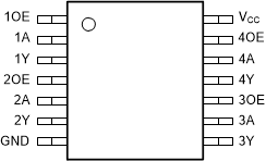
4 Pin Configuration and Functions
 Figure 4-1 PW Package, 14-Pin (Top
View)
 Figure 4-2 BQA Package, WQFN 14-Pin
(Transparent Top View)
Figure 4-2 BQA Package, WQFN 14-Pin
(Transparent Top View)Table 4-1 Pin Functions
| PIN | TYPE(1) | DESCRIPTION | |
|---|---|---|---|
| NAME | NO. | ||
| 1OE | 1 | I | Channel 1, output enable |
| 1A | 2 | I | Channel 1, A input |
| 1Y | 3 | O | Channel 1, Y output |
| 2OE | 4 | I | Channel 2, output enable |
| 2A | 5 | I | Channel 2, A input |
| 2Y | 6 | O | Channel 2, Y output |
| GND | 7 | G | Ground |
| 3Y | 8 | O | Channel 3, Y output |
| 3A | 9 | I | Channel 3, A input |
| 3OE | 10 | I | Channel 3, OE input |
| 4Y | 11 | O | Channel 4, Y output |
| 4A | 12 | I | Channel 4, A input |
| 4OE | 13 | I | Channel 4, OE input |
| VCC | 14 | P | Positive supply |
| Thermal Pad(2) | — | Thermal pad; connect to GND or leave floating | |
(1) I = input, O = output, P = power, G = ground
(2) BQA package only