-
SN74AUC1G17 Single Schmitt-Trigger Buffer
Package Options
Refer to the PDF data sheet for device specific package drawings
Mechanical Data (Package|Pins)
- DBV|5
- DCK|5
- DRL|5
- YZP|5
Thermal pad, mechanical data (Package|Pins)
Orderable Information
SN74AUC1G17 Single Schmitt-Trigger Buffer
1 Features
- Latch-Up Performance Exceeds 100 mA Per JESD 78, Class II
- ESD Protection Exceeds JESD 22
- 2000-V Human-Body Model (A114-A)
- 200-V Machine Model (A115-A)
- 1000-V Charged-Device Model (C101)
- Available in the Texas Instruments NanoFree™ Package
- Optimized for 1.8-V Operation and Is 3.6-V I/O Tolerant to Support Mixed-Mode Signal Operation
- Ioff Supports Partial Power Down Mode and Back Drive Protection
- Sub 1-V Operable
- Maximum tpd of 2.4 ns at 1.8 V
- Low Power Consumption, 10-µA Maximum ICC
- ±8-mA Output Drive at 1.8 V
2 Applications
- AV Receiver
- Audio Dock: Portable
- Blu-Ray Player and Home Theater
- Embedded PC
- MP3 Player/Recorder (Portable Audio)
- Personal Digital Assistant (PDA)
- Power: Telecom/Server AC/DC Supply: Single Controller: Analog and Digital
- Solid State Drive (SSD): Client and Enterprise
- TV: LCD/Digital and High-Definition (HDTV)
- Tablet: Enterprise
- Video Analytics: Server
- Wireless Headset, Keyboard, and Mouse
3 Description
This single Schmitt-trigger buffer is operational at 0.8-V to 2.7-V VCC, but is designed specifically for 1.65-V to 1.95-V VCC operation.
The SN74AUC1G17 contains one buffer and performs the Boolean function Y = A. The device functions as an independent buffer, but because of Schmitt action, it may have different input threshold levels for positive-going (VT+) and negative-going (VT–) signals.
NanoFree™ package technology is a major breakthrough in IC packaging concepts, using the die as the package.
This device is fully specified for partial-power-down applications using Ioff. The Ioff circuitry disables the outputs, preventing damaging current backflow through the device when it is powered down.
For more information about AUC Little Logic devices, see Applications of Texas Instruments AUC Sub-1-V Little Logic Devices, SCEA027.
Device Information(1)
| PART NUMBER | PACKAGE | BODY SIZE (NOM) |
|---|---|---|
| SN74AUC1G17DBV | SOT-23 (5) | 2.90 mm × 1.60 mm |
| SN74AUC1G17DCK | SC70 (5) | 2.00 mm × 1.25 mm |
| SN74AUC1G17DRL | SOT-5X3 (5) | 1.60 mm × 1.20 mm |
| SN74AUC1G17YZP | DSBGA (5) | 1.75 mm × 1.25 mm |
- For all available packages, see the orderable addendum at the end of the data sheet.
Logic Diagram (Positive Logic)

4 Revision History
Changes from N Revision (April 2007) to O Revision
- Deleted DRY package throughout data sheetGo
- Added Applications, Device Information table, Pin Configuration and Functions, ESD Ratings table, Thermal Information table, Feature Description section, Device Functional Modes, Device and Documentation Support section, and Mechanical, Packaging, and Orderable Information sectionGo
- Deleted Ordering Information table, see Mechanical, Packaging, and Orderable Information at the end of the data sheet Go
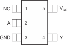
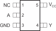
5 Pin Configuration and Functions


Pin Functions
| PIN | I/O | DESCRIPTION | ||
|---|---|---|---|---|
| NAME | DBV, DCK, DRL | YZP | ||
| A | 2 | B1 | I | A logic input |
| DNU | — | A1 | — | Do not use |
| GND | 3 | C1 | — | Ground |
| NC | 1 | — | — | No internal connection |
| VCC | 5 | A2 | — | Positive supply |
| Y | 4 | C2 | O | Y buffered output |