SCES376O SEPTEMBER 2001 – June 2017 SN74AUC1G17
UNLESS OTHERWISE NOTED, this document contains PRODUCTION DATA.
- 1 Features
- 2 Applications
- 3 Description
- 4 Revision History
- 5 Pin Configuration and Functions
- 6 Specifications
- 7 Parameter Measurement Information
- 8 Detailed Description
- 9 Device and Documentation Support
- 10Mechanical, Packaging, and Orderable Information
Package Options
Refer to the PDF data sheet for device specific package drawings
Mechanical Data (Package|Pins)
- DBV|5
- DCK|5
- DRL|5
- YZP|5
Thermal pad, mechanical data (Package|Pins)
Orderable Information
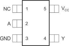
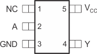
5 Pin Configuration and Functions
DBV Package
5-Pin SOT-23
Top View

DCK Package
5-Pin SC70
Top View

See mechanical drawings for dimensions.
NC – No internal connection
DNU – Do not use
DRL Package
5-Pin SOT-5X3
Top View

YZP Package
5-Pin DSBGA
Bottom View

Pin Functions
| PIN | I/O | DESCRIPTION | ||
|---|---|---|---|---|
| NAME | DBV, DCK, DRL | YZP | ||
| A | 2 | B1 | I | A logic input |
| DNU | — | A1 | — | Do not use |
| GND | 3 | C1 | — | Ground |
| NC | 1 | — | — | No internal connection |
| VCC | 5 | A2 | — | Positive supply |
| Y | 4 | C2 | O | Y buffered output |