SCLS115G December 1982 – September 2015 SN54HC164 , SN74HC164
PRODUCTION DATA.
- 1 Features
- 2 Applications
- 3 Description
- 4 Revision History
- 5 Device Comparison Table
- 6 Pin Configuration and Functions
-
7 Specifications
- 7.1 Absolute Maximum Ratings
- 7.2 ESD Ratings
- 7.3 Recommended Operating Conditions
- 7.4 Thermal Information
- 7.5 Electrical Characteristics, TA = 25°C
- 7.6 Electrical Characteristics, TA = -55°C to 125°C
- 7.7 Electrical Characteristics, TA = -55°C to 85°C
- 7.8 Timing Requirements, TA = 25°C
- 7.9 Timing Requirements, TA = -55°C to 125°C
- 7.10 Timing Requirements, TA = -55°C to 85°C
- 7.11 Switching Characteristics, TA = 25°C
- 7.12 Switching Characteristics, TA = -55°C to 125°C
- 7.13 Switching Characteristics, TA = -55°C to 85°C
- 8 Parameter Measurement Information
- 9 Detailed Description
- 10Application and Implementation
- 11Power Supply Recommendations
- 12Layout
- 13Device and Documentation Support
- 14Mechanical, Packaging, and Orderable Information
Package Options
Refer to the PDF data sheet for device specific package drawings
Mechanical Data (Package|Pins)
- D|14
- PW|14
- N|14
- NS|14
Thermal pad, mechanical data (Package|Pins)
Orderable Information
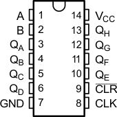
6 Pin Configuration and Functions
D, N, NS, J, W, or PW Package
14-Pin SOIC, PDIP, SO, CDIP, CFP, or TSSOP
Top View

Pin Functions
| PIN | I/O | DESCRIPTION | |
|---|---|---|---|
| SOIC, PDIP, SO, CDIP, CFP, or TSSOP NO. | NAME | ||
| 1 | A | I | Gated Serial Input 1 |
| 2 | B | I | Gated Serial Input 2 |
| 3 | QA | O | Parallel Output |
| 4 | QB | O | Parallel Output |
| 5 | QC | O | Parallel Output |
| 6 | QD | O | Parallel Output |
| 7 | GND | - | Ground |
| 8 | CLK | I | Clock |
| 9 | CLR | I | Clear 1 Active-Low |
| 10 | QE | O | Parallel Output |
| 11 | QF | O | Parallel Output |
| 12 | QG | O | Parallel Output |
| 13 | QH | O | Parallel Output |
| 14 | VCC | — | Power |
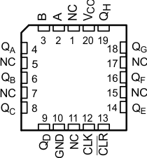
FK Package
20-Pin LCCC
Top View

NC – No internal connection
Pin Functions
| PIN | I/O | DESCRIPTION | |
|---|---|---|---|
| LCCC NO. | NAME | ||
| 1 | NC | — | No Connect |
| 2 | A | I | Gated Serial Input 1 |
| 3 | B | I | Gated Serial Input 2 |
| 4 | QA | O | Parallel Output |
| 5 | NC | — | No Connect |
| 6 | QB | O | Parallel Output |
| 7 | NC | — | No Connect |
| 8 | QC | O | Parallel Output |
| 9 | QD | O | Parallel Output |
| 10 | GND | — | Ground |
| 11 | NC | — | No Connect |
| 12 | CLK | I | Clock |
| 13 | CLR | I | Clear 1 Active-Low |
| 14 | QE | O | Parallel Output |
| 15 | NC | — | No Connect |
| 16 | QF | O | Parallel Output |
| 17 | NC | — | No Connect |
| 18 | QG | O | Parallel Output |
| 19 | QH | O | Parallel Output |
| 20 | VCC | — | Power |