SCLS393Q APRIL 1998 – August 2015 SN74LV123A
UNLESS OTHERWISE NOTED, this document contains PRODUCTION DATA.
- 1 Features
- 2 Applications
- 3 Description
- 4 Revision History
- 5 Description (continued)
- 6 Pin Configuration and Functions
-
7 Specifications
- 7.1 Absolute Maximum Ratings
- 7.2 ESD Ratings
- 7.3 Recommended Operating Conditions
- 7.4 Thermal Information
- 7.5 Electrical Characteristics
- 7.6 Timing Requirements, VCC = 2.5 V ± 0.2 V
- 7.7 Timing Requirements, VCC = 3.3 V ± 0.3 V
- 7.8 Timing Requirements, VCC = 5 V ± 0.5 V
- 7.9 Switching Characteristics, VCC = 2.5 V ± 0.2 V
- 7.10 Switching Characteristics, VCC = 3.3 V ± 0.3 V
- 7.11 Switching Characteristics, VCC = 5 V ± 0.5 V
- 7.12 Operating Characteristics
- 7.13 Typical Characteristics
- 8 Parameter Measurement Information
- 9 Detailed Description
- 10Application and Implementation
- 11Power Supply Recommendations
- 12Layout
- 13Device and Documentation Support
- 14Mechanical, Packaging, and Orderable Information
Package Options
Mechanical Data (Package|Pins)
Thermal pad, mechanical data (Package|Pins)
- RGY|16
Orderable Information
10 Application and Implementation
NOTE
Information in the following applications sections is not part of the TI component specification, and TI does not warrant its accuracy or completeness. TI’s customers are responsible for determining suitability of components for their purposes. Customers should validate and test their design implementation to confirm system functionality.
10.1 Application Information
The SNx4LV123A device is a dual monostable multivibrator. It can be configured for many pulse width outputs and rising- or falling-edge triggering. The application shown here could be used to signal separate interruptable inputs on a microcontroller when an input had a rising or falling edge.
10.2 Typical Application
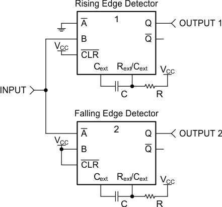 Figure 8. Simplified Application Schematic
10.2.1 Design Requirements
CAUTION
To prevent malfunctions due to noise, connect a high-frequency capacitor between VCC and GND, and keep the wiring between the external components and Cext and Rext/Cext terminals as short as possible.
10.2.1.1 Power-Down Considerations
Large values of Cext can cause problems when powering down the 'LV123A devices because of the amount of energy stored in the capacitor. When a system containing this device is powered down, the capacitor can discharge from VCC through the protection diodes at pin 2 or pin 14. Current through the input protection diodes must be limited to 30 mA; therefore, the turn-off time of the VCC power supply must not be faster than t = VCC × Cext/30 mA. For example, if VCC = 5 V and Cext = 15 pF, the VCC supply must turn off no faster than t = (5 V) × (15 pF)/30 mA = 2.5 ns. Usually, this is not a problem because power supplies are heavily filtered and cannot discharge at this rate. When a more rapid decrease of VCC to zero occurs, the 'LV123A devices can sustain damage. To avoid this possibility, use external clamping diodes.
10.2.1.2 Output Pulse Duration
The output pulse duration, tw, is determined primarily by the values of the external capacitance (CT) and timing resistance (RT). The timing components are connected as shown in Figure 9.
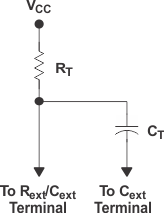 Figure 9. Timing-Component Connections
If CT is ≥1000 pF and K = 1.0, the pulse duration is given by:
where
- tw = pulse duration in ns
- RT = external timing resistance in kΩ
- CT = external capacitance in pF
- K = multiplier factor
if CT is <1000 pF, K can be determined from Figure 3
Equation 1 and Figure 13 can be used to determine values for pulse duration, external resistance, and external capacitance.
10.2.1.3 Retriggering Data
The minimum input retriggering time (tMIR) is the minimum time required after the initial signal before retriggering the input. After tMIR, the device retriggers the output. Experimentally, it also can be shown that to retrigger the output pulse, the two adjacent input signals must be tMIR apart, where tMIR = 0.30 × tw. The retrigger pulse duration is calculated as shown in Figure 10.
 Figure 10. Retrigger Pulse Duration
The minimum value from the end of the input pulse to the beginning of the retriggered output must be approximately 15 ns to ensure a retriggered output (see Figure 11).
 Figure 11. Input and Output Requirements
10.2.2 Detailed Design Procedure
- Timing requirements:
- The pulse width must be long enough to be read by the desired output system, but short enough so that the output pulse completes prior to the next trigger event. It is recommended to make the output pulse just 10% longer than the minimum required for the output system.
- Recommended input conditions:
- Slow or noisy inputs are allowed on A, B, and CLR due to Schmitt-trigger input circuitry.
- Specified high and low levels. See (VIH and VIL) in Recommended Operating Conditions.
- Recommended output conditions:
- Load currents must not exceed the values listed in Absolute Maximum Ratings.
10.2.3 Application Curves
Operation of the devices at these or any other conditions beyond those indicated under Recommended Operating Conditions is not implied.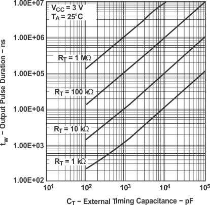 Figure 12. Output Pulse Duration vs. External Timing Capacitance
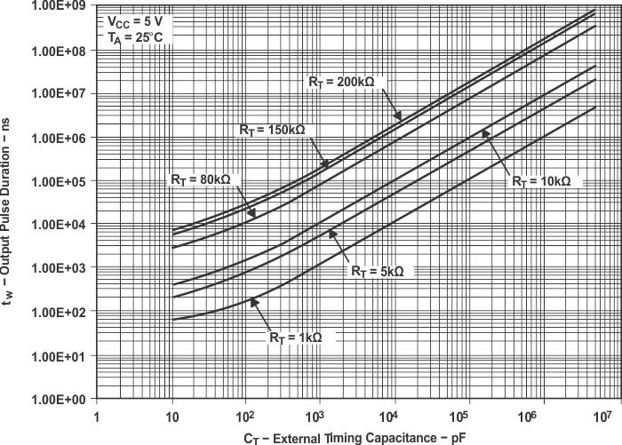 Figure 14. Output Pulse Duration
 vs External Timing Capacitance
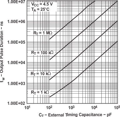 Figure 13. Output Pulse Duration vs. External Timing Capacitance
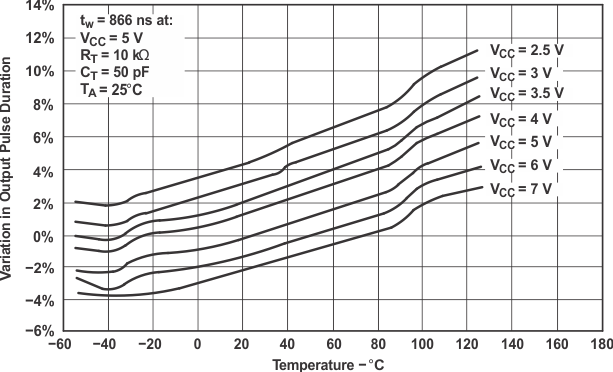
vs Temperature