SCLS986 November 2023 SN74LV2T74-EP
PRODUCTION DATA
- 1
- 1 Features
- 2 Applications
- 3 Description
- 4 Pin Configuration and Functions
- 5 Specifications
- 6 Parameter Measurement Information
- 7 Detailed Description
- 8 Application and Implementation
- 9 Device and Documentation Support
- 10Revision History
- 11Mechanical, Packaging, and Orderable Information
Package Options
Refer to the PDF data sheet for device specific package drawings
Mechanical Data (Package|Pins)
- PW|14
Thermal pad, mechanical data (Package|Pins)
Orderable Information
4 Pin Configuration and Functions
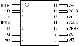
 Figure 4-1 PW Package, 14-Pin TSSOP
(Top View)
Figure 4-1 PW Package, 14-Pin TSSOP
(Top View)Table 4-1 Pin Functions
| PIN | TYPE | DESCRIPTION | |
|---|---|---|---|
| NAME | NO. | ||
| 1CLR | 1 | Input | Clear for channel 1, active low |
| 1D | 2 | Input | Data for channel 1 |
| 1CLK | 3 | Input | Clock for channel 1, rising edge triggered |
| 1PRE | 4 | Input | Preset for channel 1, active low |
| 1Q | 5 | Output | Output for channel 1 |
| 1Q | 6 | Output | Inverted output for channel 1 |
| GND | 7 | — | Ground |
| 2Q | 8 | Output | Inverted output for channel 2 |
| 2Q | 9 | Output | Output for channel 2 |
| 2PRE | 10 | Input | Preset for channel 2, active low |
| 2CLK | 11 | Input | Clock for channel 2, rising edge triggered |
| 2D | 12 | Input | Data for channel 2 |
| 2CLR | 13 | Input | Clear for channel 2, active low |
| VCC | 14 | — | Positive supply |