SCAS292S January 1993 – December 2024 SN54LVC157A , SN74LVC157A
PRODUCTION DATA
- 1
- 1 Features
- 2 Description
- 3 Pin Configuration and Functions
-
4 Specifications
- 4.1 Absolute Maximum Ratings
- 4.2 ESD Ratings
- 4.3 Recommended Operating Conditions, SN54LVC157A
- 4.4 Recommended Operating Conditions, SN74LVC157A
- 4.5 Thermal Information
- 4.6 Electrical Characteristics, SN54LVC157A
- 4.7 Electrical Characteristics, SN74LVC157A
- 4.8 Switching Characteristics, SN54LVC157A
- 4.9 Switching Characteristics, SN74LVC157A
- 4.10 Operating Characteristics
- 5 Parameter Measurement Information
- 6 Detailed Description
- 7 Application and Implementation
- 8 Device and Documentation Support
- 9 Revision History
- 10Mechanical, Packaging, and Orderable Information
Package Options
Mechanical Data (Package|Pins)
Thermal pad, mechanical data (Package|Pins)
Orderable Information
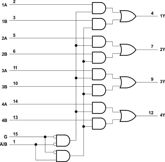
6.2 Functional Block Diagram

Pin numbers shown
are for the D, DB, DGV, J, N, NS, PW, RGY, and W packages.
Figure 6-1 Logic Diagram (Positive
Logic)