SLLS059E February 1990 – February 2024 SN751177 , SN751178
PRODUCTION DATA
- 1
- 1 Features
- 2 Applications
- 3 Description
- 4 Pin Configuration and Functions
- 5 Specifications
- 6 Parameter Measurement Information
- 7 Detailed Description
- 8 Device and Documentation Support
- 9 Revision History
- 10Mechanical, Packaging, and Orderable Information
Package Options
Refer to the PDF data sheet for device specific package drawings
Mechanical Data (Package|Pins)
- NS|16
- N|16
Thermal pad, mechanical data (Package|Pins)
Orderable Information
7.1 Device Functional Modes
Table 7-1 SN751177, SN751178 Functional
Table (Each Driver)
| INPUT D(1) | ENABLE DE | OUTPUTS | |
|---|---|---|---|
| Y | Z | ||
| H | H | H | L |
| L | H | L | H |
| X | L | Z | Z |
(1) H = high level, L = low level, X = irrelevant, Z =
high impedance (off)
Table 7-2 SN751177 Functional Table
(Each Receiver)
| DIFFERENTIAL INPUTS A − B | ENABLE RE | OUTPUT R(1) |
|---|---|---|
| VID ≥ 0.2V | L | H |
| −0.2V < VID < 0.2V | L | ? |
| VID ≤ −0.2V | L | L |
| X | H | Z |
| Open | L | H |
(1) H = high level, L = low level, ? = indeterminate, X =
irrelevant, Z = high impedance (off)
Table 7-3 SN751178 Functional Table
(Each Receiver)
| DIFFERENTIAL INPUTS A − B | OUTPUT R(1) |
|---|---|
| VID ≥ 0.2V | H |
| −0.2V < VID < 0.2V | ? |
| VID ≤ −0.2V | L |
(1) H = high level, L = low level, ? = indeterminate

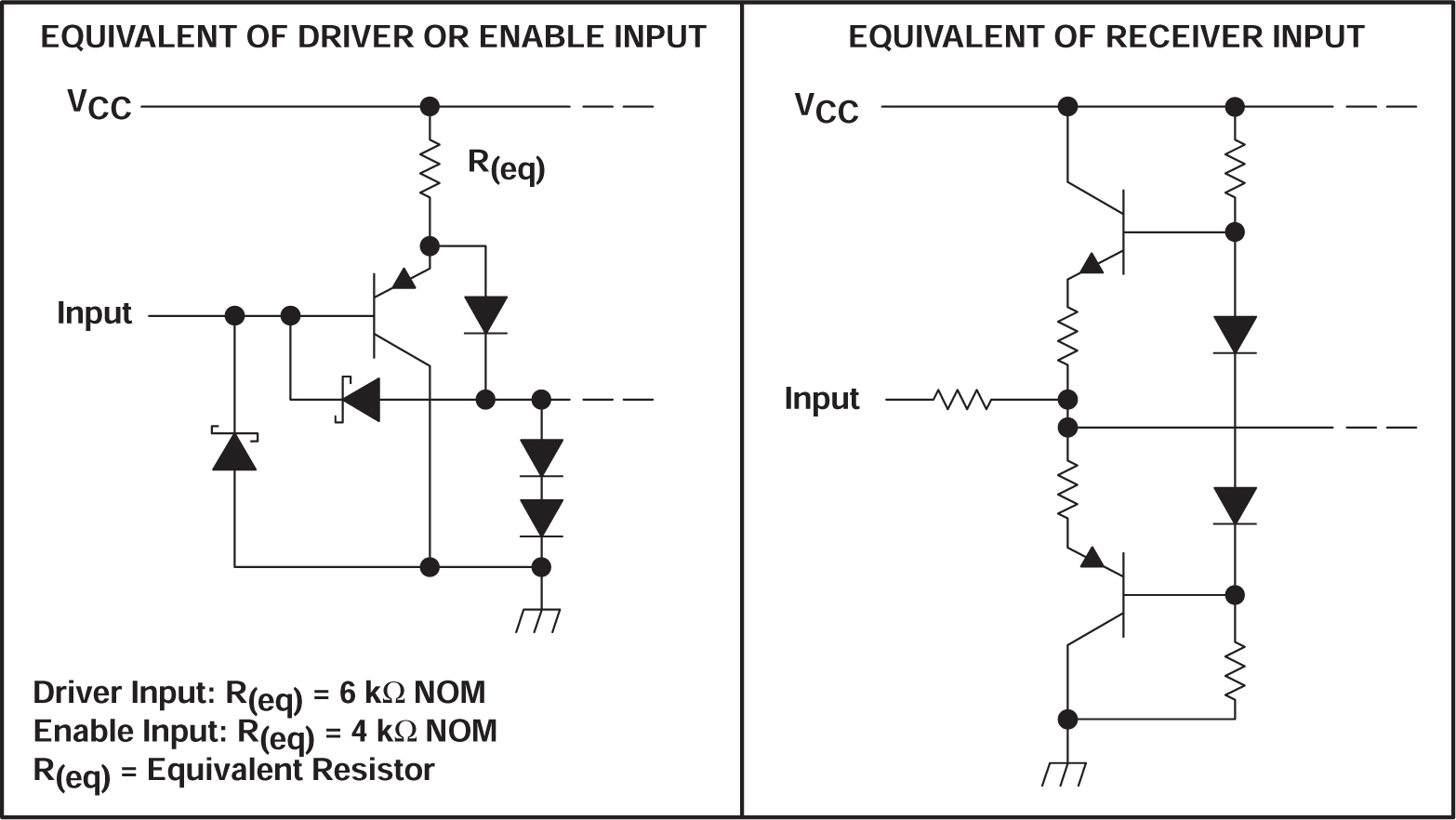
A. All resistor
values are nominal.
Figure 7-1 Schematics of Inputs
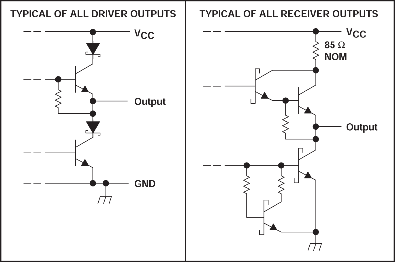
A. All resistor
values are nominal.
Figure 7-2 Schematics of Outputs