SLLS040I August 1987 – January 2023 SN65ALS176 , SN75ALS176 , SN75ALS176A , SN75ALS176B
PRODUCTION DATA
- 1 Features
- 2 Description
- 3 Revision History
- 4 Pin Configuration and Functions
-
5 Specifications
- 5.1 Absolute Maximum Ratings
- 5.2 Recommended Operating Conditions
- 5.3 Thermal Information
- 5.4 Electrical Characteristics - Driver
- 5.5 Switching Characteristics - Driver
- 5.6 Switching Characteristics - Driver
- 5.7 Symbol Equivalents
- 5.8 Electrical Characteristics - Receiver
- 5.9 Switching Characteristics - Receiver
- 5.10 Switching Characteristics - Receiver
- 5.11 Typical Characteristics
- 6 Parameter Measurement Information
- 7 Detailed Description
- 8 Application and Implementation
- 9 Device and Documentation Support
- 10Mechanical, Packaging, and Orderable Information
Package Options
Refer to the PDF data sheet for device specific package drawings
Mechanical Data (Package|Pins)
- D|8
- P|8
Thermal pad, mechanical data (Package|Pins)
Orderable Information
5.11 Typical Characteristics
Operation of the device at these or any other conditions beyond those indicated under ‘‘recommended operating conditions” is not implied.
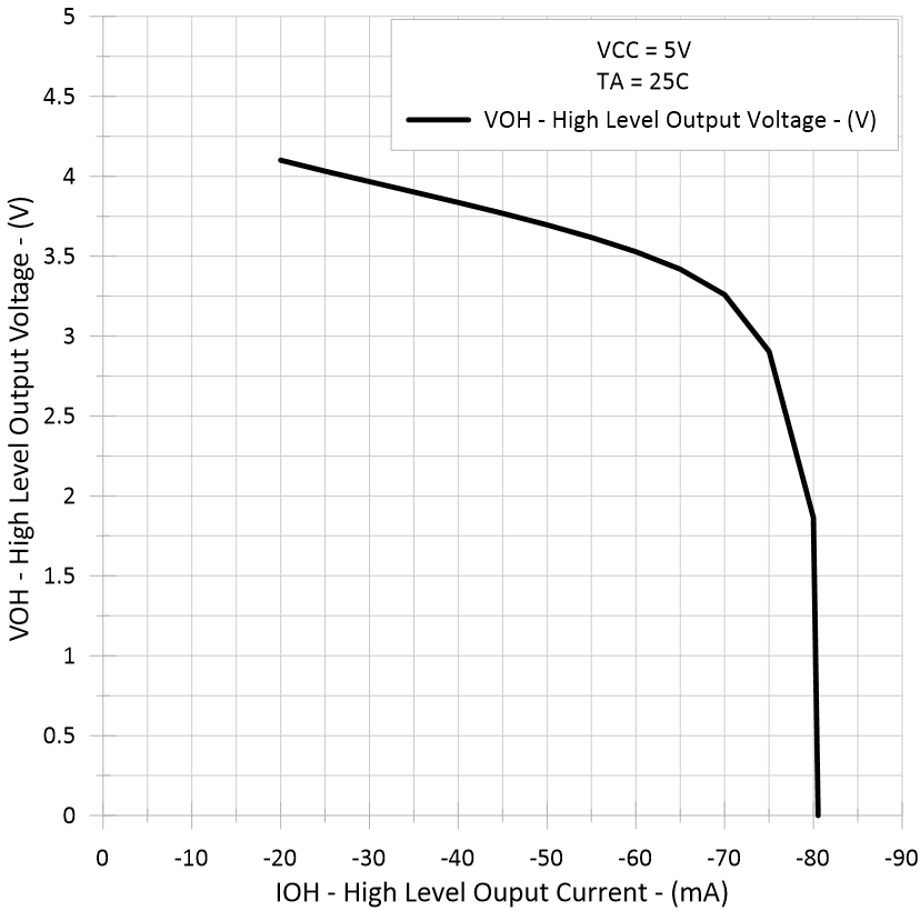 Figure 5-1 Driver High-LeveL Output Voltage vs High-Level Output Current
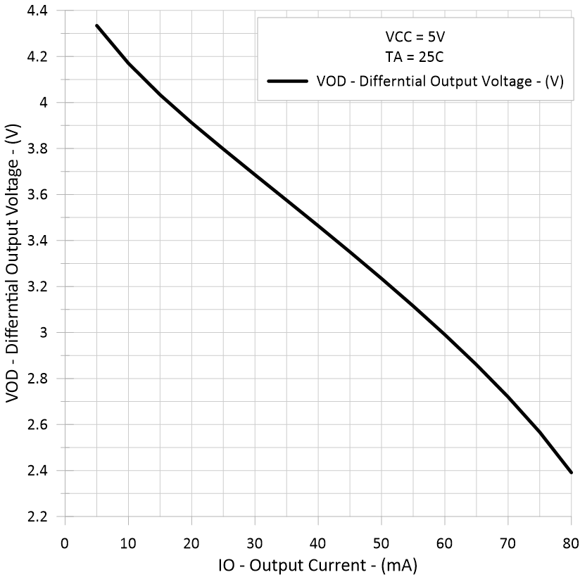 Figure 5-3 Driver Differential Output Voltage vs Output Current
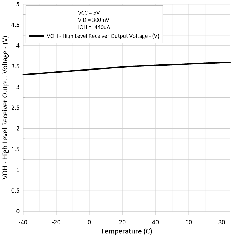 Figure 5-5 Receiver High-Level Output Voltage vs Free-Air Temperature
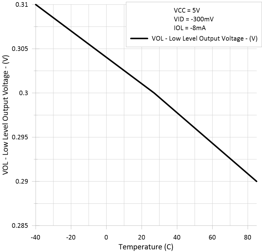 Figure 5-7 Receiver Low-Level Output
Voltage vs Free-Air Temperature
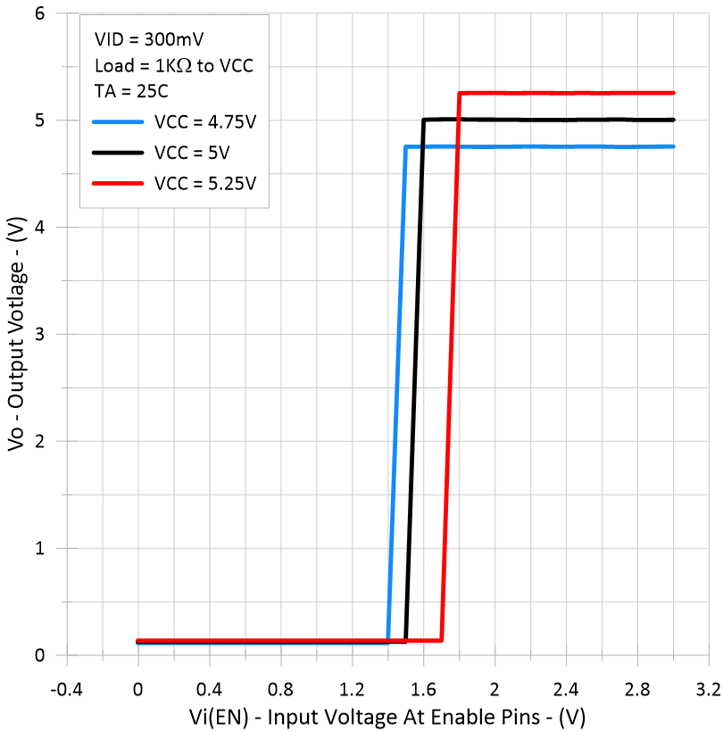 Figure 5-9 Receiver Output Voltage vs
Enable Voltage
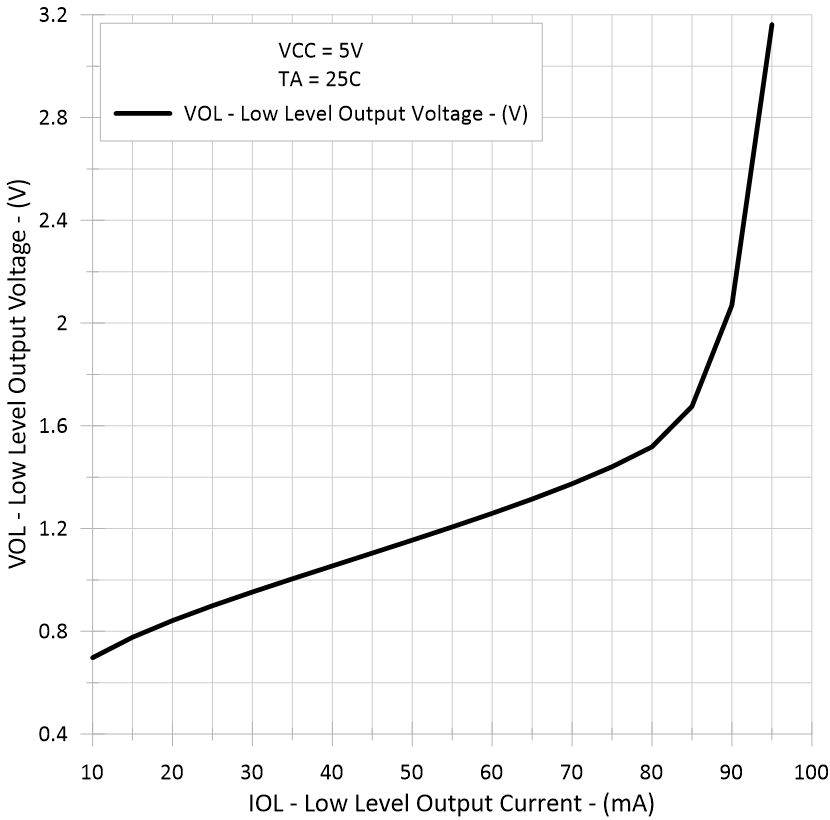 Figure 5-2 Driver Low-Level Output Voltage vs Low-Level Output Current
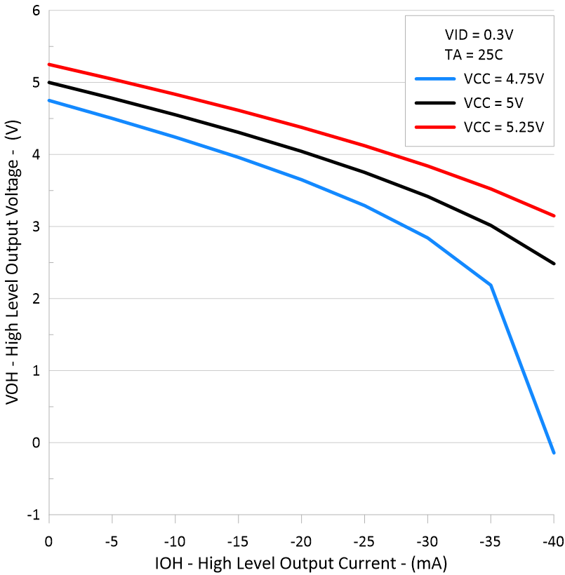 Figure 5-4 Receiver High-Level Output Voltage vs High-Level Output Current
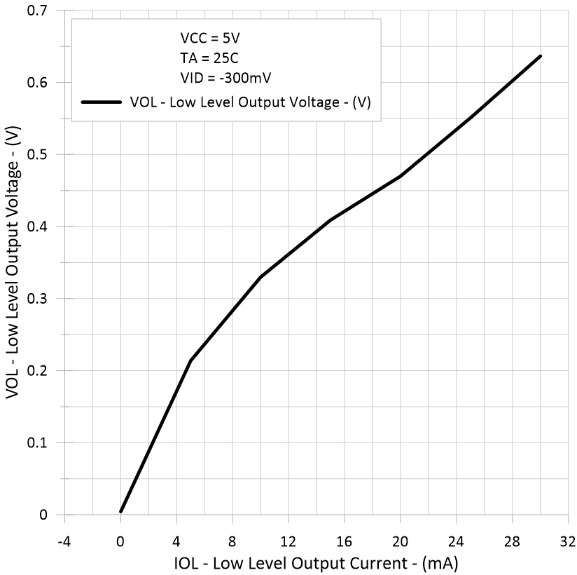 Figure 5-6 Receiver Low-Level Output Voltage vs Low-Level Output Current
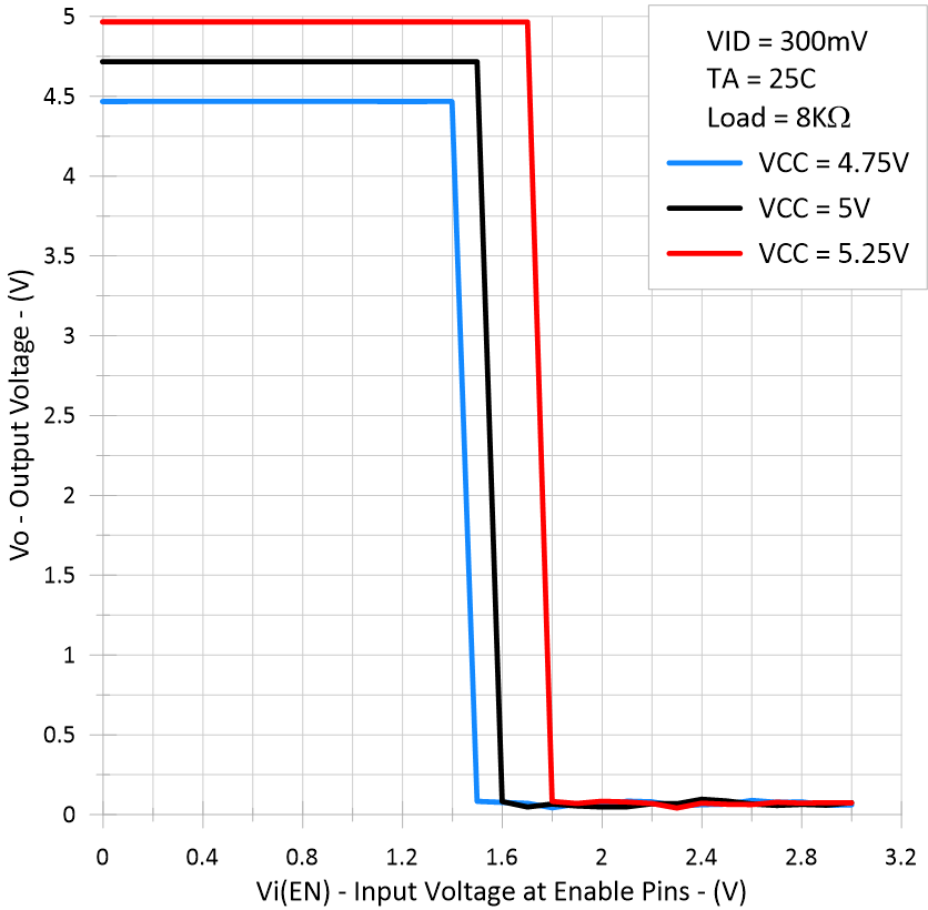 Figure 5-8 Receiver Output Voltage vs
Enable Voltage