SLLSE57E April 2011 – March 2015 SN75DP130
PRODUCTION DATA.
- 1 Features
- 2 Applications
- 3 Description
- 4 Revision History
- 5 Description (continued)
- 6 Pin Configuration and Functions
- 7 Specifications
- 8 Parameter Measurement Information
- 9 Detailed Description
- 10Application and Implementation
- 11Power Supply Recommendations
- 12Layout
- 13Device and Documentation Support
- 14Mechanical, Packaging, and Orderable Information
Package Options
Mechanical Data (Package|Pins)
- RGZ|48
Thermal pad, mechanical data (Package|Pins)
- RGZ|48
Orderable Information
7 Specifications
7.1 Absolute Maximum Ratings
over operating free-air temperature range (unless otherwise noted) (1)| MIN | MAX | UNIT | |||
|---|---|---|---|---|---|
| Supply voltage | VCC | –0.3 | 4 | V | |
| VDDD, VDDD_DREG | –0.3 | 1.3 | |||
| Voltage | Main link I/O differential voltage | –0.3 | 1.3 | V | |
| HPD_SNK | –0.3 | 5.5 | |||
| All other terminals | –0.3 | 4 | |||
| Storage temperature, Tstg | –65 | 150 | °C | ||
(1) Stresses beyond those listed under Absolute Maximum Ratings may cause permanent damage to the device. These are stress ratings only, which do not imply functional operation of the device at these or any other conditions beyond those indicated under Recommended Operating Conditions. Exposure to absolute-maximum-rated conditions for extended periods may affect device reliability.
7.2 ESD Ratings
| VALUE | UNIT | |||
|---|---|---|---|---|
| V(ESD) | Electrostatic discharge | Human-body model (HBM), per ANSI/ESDA/JEDEC JS-001(1) | ±2000 | V |
| Charged-device model (CDM), per JEDEC specification JESD22-C101(2) | ±500 | |||
(1) JEDEC document JEP155 states that 500-V HBM allows safe manufacturing with a standard ESD control process.
(2) JEDEC document JEP157 states that 250-V CDM allows safe manufacturing with a standard ESD control process.
7.3 Recommended Operating Conditions
7.4 Thermal Information
| THERMAL METRIC(1) | SN75DP130 | UNIT | |
|---|---|---|---|
| RGZ (VQFN) | |||
| 48 PINS | |||
| RθJA | Junction-to-ambient thermal resistance | 35.1 | °C/W |
| RθJCtop | Junction-to-case (top) thermal resistance | 21.5 | |
| RθJB | Junction-to-board thermal resistance | 11.7 | |
| ψJT | Junction-to-top characterization parameter, high-k board | 1.2 | |
| ψJB | Junction-to-board characterization parameter, high-k board | 11.9 | |
| RθJCbot | Junction-to-case (bottom) thermal resistance | 6.7 | |
(1) For more information about traditional and new thermal metrics, see the IC Package Thermal Metrics application report, SPRA953.
7.5 Power Dissipation
See SN75DP130 Power Sequencing.| PARAMETER | TEST CONDITIONS(1) | MIN | TYP | MAX | UNIT | |
|---|---|---|---|---|---|---|
| PN | Device power under normal operation | SN75DP130SS; 4 DP Lanes. | 468 | 828 | mW | |
| SN75DP130DS; 4 DP Lanes. | 174 | 304 | ||||
| SN75DP130SS; 2 DP Lanes | 252 | 450 | ||||
| SN75DP130DS; 2 DP Lanes. | 102 | 178 | ||||
| SN75DP130SS; 1 DP Lanes | 144 | 252 | ||||
| SN75DP130DS; 1 DP Lanes. | 66 | 112 | ||||
| PSD | Shutdown mode power dissipation | SN75DP130SS; 4 DP Lanes. | 14.4 | mW | ||
| SN75DP130DS; 4 DP Lanes. | 7.2 | |||||
| PSBY | Standby mode power dissipation | SN75DP130SS; 4 DP Lanes. | 14.4 | mW | ||
| SN75DP130DS; 4 DP Lanes. | 7.2 | |||||
| PD3 | D3 power down mode dissipation | SN75DP130SS; 4 DP Lanes. | 54 | mW | ||
| SN75DP130DS; 4 DP Lanes. | 46 | |||||
| POD | Output disable (squelch) mode current | SN75DP130SS; 4 DP Lanes. | 126 | 180 | mW | |
| SN75DP130DS; 4 DP Lanes. | 58 | 88 | ||||
(1) Test conditions correspond to Power Supply test conditions in Electrical Characteristics
7.6 Electrical Characteristics
over recommended operating conditions (unless otherwise noted)| PARAMETER(1) | TEST CONDITIONS | MIN | TYP | MAX | UNIT | |
|---|---|---|---|---|---|---|
| POWER SUPPLY | ||||||
| ICCDP1HBR2 | Supply Current 1 DP Lanes | Maximum conditions: IN/OUT at 5.4 Gbps PRBS,VOD = 510 mVpp, PE = 6 dB; AUX at 1 Mbps PRBS, VID = 1000 mVpp; EQ = 3.5 dB Typical Conditions: IN/OUT at 5.4 Gbps PRBS,VOD = 510 mVpp, PE = 0dB AUX and I2C Idle; EQ = 5 3dB |
40 | 70 | mA | |
| ICCDP2HBR2 | Supply Current 2 DP Lanes | 70 | 125 | mA | ||
| ICCDP4HBR2 | Supply Current 4 DP Lanes | 130 | 230 | mA | ||
| ICCDP1HBR | Supply Current 1 DP Lanes | Main Link at 2.7Gbps PRBS, VOD = 510 mVpp, PE = 0 dB; AUX and I2C Idle; EQ at 3 dB fixed gain |
40 | mA | ||
| ICCDP2HBR | Supply Current 2 DP Lanes | 70 | mA | |||
| ICCDP4HBR | Supply Current 4 DP Lanes | 130 | mA | |||
| ICCTMDS | Supply Current TMDS Mode | Main Link at 2.5 Gbps PRBS, VID = VOD = 600 mVpp; AUX Idle |
170 | mA | ||
| ISD | Shutdown supply current | Shutdown mode | 3 | 4 | mA | |
| ISBY | Standby supply current | Standby mode | 3 | 4 | mA | |
| ID3 | D3 supply current | D3 power-down mode | 10 | 15 | mA | |
| IOD | Squelch supply current | Output disable (Squelch) mode | 35 | 50 | mA | |
| MAIN LINK | ||||||
| VOD(L0) | Output differential voltage swing | VPRE(L0); 675 Mbps D10.2 Test Pattern; BOOST = 01 | 238 | 340 | 442 | mVPP |
| VOD(L1) | 357 | 510 | 663 | |||
| VOD(L2) | 484 | 690 | 897 | |||
| VOD(L3) | 700 | 1000 | 1300 | |||
| VOD(TMDS) | 675 Mbps D10.2 Test Pattern; BOOST = 01 | 420 | 600 | 780 | ||
| ΔVOD(L0L1) | Output peak-to-peak differential voltage delta | ΔVODn = 20×log(VODL(n+1) / VODL(n)) measured in compliance with PHY CTS1.1D15 section 3.2 at test point TP2 using special CTS test board | 1.7 | 3.5 | 5.3 | dB |
| ΔVOD(L1L2) | 1.6 | 2.5 | 3.5 | |||
| ΔVOD(L2L3) | 0.8 | 3.5 | 6 | |||
| VPRE(L0) | Driver output pre-emphasis (default) | All VOD options | 0 | 0.25 | dB | |
| VPRE(L1) | VOD = VOD(L0), VOD(L1), or VOD(L2); BOOST = 01 | 3.5 | ||||
| VPRE(L2) | VOD = VOD(L0) or VOD(L1); BOOST = 01 | 6 | ||||
| VPRE(L3) | VOD = VOD(L0); BOOST = 01 | 9.5 | ||||
| VPRE(BOOST) | Output VPRE boost | BOOST = 10 | 10% | dB | ||
| BOOST = 00 | –10% | |||||
| ΔVPRE(L1L0) | Pre-emphasis delta | Measured in compliance with PHY CTS1.1D15 section 3.3 at test point TP2 using special CTS test board | 2 | dB | ||
| ΔVPRE(L2L1) | 1.6 | |||||
| ΔVPRE(L3L2) | 1.6 | |||||
| ΔVConsBit | Nontransition bit voltage variation | See CTS spec section 3.3.5 | 30% | |||
| AEQ(HBR) | Equalizer gain for RBR/HBR | See Table 3 for EQ setting details; Max value represents the typical value for the maximum configurable EQ setting |
9 | dB | ||
| AEQ(HBR2) | Equalizer gain for HBR2 | 18 | dB | |||
| AEQ(TMDS) | Equalizer gain for TMDS | 3 | dB | |||
| ROUT | Driver output impedance | 50 | Ω | |||
| RIN | Input termination impedance | 40 | 50 | 60 | Ω | |
| VIterm | Input termination voltage | AC coupled; self-biased | 0 | 2 | V | |
| VOCM(SS) | Steady state output common-mode voltage | 0 | 2 | V | ||
| ΔVOCM(SS) | Change in steady state output common-mode voltage between logic levels | Tested in compliance to section 3.10 in CTS 1.1a | 10 | mVPP | ||
| VOCM(PP) | Output common-mode noise | HBR2 | 20 | mVRMS | ||
| 30 | ||||||
| VSQUELCH | Squelch threshold voltage | Programable through I2C; default at 80 mVpp typical | 80 | mVPP | ||
| ITXSHORT | Short circuit current limit | Main Link outputs shorted to GND | 50 | mA | ||
| HPD_SRC, CAD_SRC | ||||||
| VOH | High-level output voltage | IOH = 500 µA | 2.7 | 3.6 | V | |
| VOL | Low-level output voltage | IOH = 500 µA | 0 | 0.1 | V | |
| RoutCAD | CAD series output resistance(2) | EN = RSTN = VCC; HPD_SNK = CAD_SNK = VCC | 150 | Ω | ||
| RoutHPD | HPD series output resistance | EN = RSTN = VCC; HPD_SNK = CAD_SNK = VCC | 150 | Ω | ||
| ILEAK | Leakage current (3) | VCC = 0 V, V(pin) = 1.2 V; RSTN | 20 | μA | ||
| VCC = 0 V, V(pin) = 3.3 V; SCL/SDA_CTL, AUX_SNKp/n | 20 | |||||
| VCC = 0 V, V(pin) = 3.3 V; HPD_SNK | 40 | |||||
| VCC = 0 V, V(pin) = 3.3 V; AUX_SRCp/n | 60 | |||||
| HPD_SNK | ||||||
| IH | High-level input current | VIH = 1.9 V (leakage includes the 130-kΩ pull-down resistor) | –30 | 30 | µA | |
| IL | Low-level input current | VIL = 0.8 V (leakage includes the 130-kΩ pull-down resistor) | –30 | 30 | µA | |
| VTH+ | Positive going input threshold voltage | 1.4 | V | |||
| RpdHPD | HPD input termination to GND | VCC = 0 V | 100 | 130 | 160 | kΩ |
| CAD_SNK | ||||||
| IH | High-level input current | VIH = 1.9 V | –1 | 1 | µA | |
| IL | Low-level input current | VIL = 0.8 V | –1 | 1 | µA | |
| VTH+ | Positive going input threshold voltage | 1.4 | V | |||
| AUX/DDC/I2C | ||||||
| VPASS | DDC mode passthrough voltage | VCAD_SNK = VIH; IO = 100 µA | 1.9 | V | ||
| CIO | I/O capacitance | VIO = 0 V; f(test) = 1 MHz | 10 | pF | ||
| rON | On resistance AUX_SRCn to AUX_SNKn in DP mode | VCC = 3 V w/ VI = 2.85 V or VCC = 3.6 V w/ VI = 3.4 V; IO = 5 mA |
5 | 10 | Ω | |
| On resistance SCL/SDA_DDC to AUX_SNK in TMDS mode | IO = 3 mA | 15 | 30 | |||
| On resistance AUX_SRC to AUX_SNK in TMDS mode | IO = 3 mA | 10 | 20 | |||
| ΔrON | On resistance variation with input signal voltage change in DP mode | VCC = 3.6 V, IO = 5 mA, VI = 2.6 to 3.4 V, VCC = 3 V, IO = 5 mA, VI = 0 to 0.4 V |
5 | Ω | ||
| VID(HYS) | Differential input hysterisis | By design (simulation only) | 50 | mV | ||
| IH | High-level input current | VI = VCC | –5 | 5 | µA | |
| IL | Low-level input current | VI = GND; CAD_SNK = VIH | –5 | 5 | µA | |
| VI = GND; At DDC inputs | 80 | |||||
| VAUX+ | Voltage on the Aux+ for PHY-CTS 3.19 | 1M (5%) pullup to VCC and 100-kΩ pulldown to GND on AUX+; VCC = 3.3 V | 0 | 0.4 | V | |
| VAUX- | Voltage on the Aux- for PHY-CTS 3.18 | 100 kΩ pullup to VCC and 1M (5%) pulldown to GND on AUX-; VCC = 3.3 V |
2.4 | 3.6 | V | |
| |S1122| | Differential line insertion loss | VID = 400 mV, AC coupled; p-channel biasing 0.3 V and N-channel 3 V; 360-MHz sine wave; CAD_SNK = VIL |
1.6 | 3 | dB | |
| RDDC | Switcheable pul-lup resistor on DDC at source side (SCL_DDC, SDA_DDC) | CAD_SNK = VIH | 48 | 60 | 72 | kΩ |
(1) Values are VDD supply measurements; VCC supply (DS package option) measurements are 5 mA (typical) and 8 mA (max), with zero current in shutdown and standby modes.
(2) A series output resistance of 100kΩ may be added in series to the CAD_SRC output to mimic a cable adapter.
(3) Applies to failsafe inputs: RSTN, SDA_CTL, SCL_CTL, SDA_DDC, SCL_DDC, AUX_SNK P/N, AUX_SRC P/N, HPD_SNK
7.7 Switching Characteristics
over recommended operating conditions (unless otherwise noted)| PARAMETER | TEST CONDITIONS | MIN | TYP | MAX | UNIT | |
|---|---|---|---|---|---|---|
| MAIN LINK | ||||||
| tPD | Propagation delay time | See Figure 10 | 300 | ps | ||
| tSK(1) | Intra-pair output skew | Signal input skew = 0ps; dR = 2.7 Gbps, VPRE = 0 dB, 800 mVp-p, D10.2 clock pattern at device input; See Figure 11 | 20 | ps | ||
| tSK(2) | Inter-pair output skew | 100 | ps | |||
| Δtjit | Total peak-to-peak residual jitter | VOD(L0); VPRE(L0); EQ = 8 dB; clean source; minimum input and output cabling; 1.62 Gbps, 2.7 Gbps, and 5.4 Gbps PRBS7 data pattern. | 15 | ps | ||
| tsq_enter | Squelch entry time | Time from active DP signal turned off to ML output off with noise floor minimized | 10 | 120 | μs | |
| tsq_exit | Squelch exit time | Time from DP signal on to ML output on | 0 | 1 | μs | |
| HPD/CAD | ||||||
| tPD(HPD) | Propagation delay HPD_SNK to HPD_SRC | VCC = 3 V; See Figure 1 | 50 | ns | ||
| tPD(CAD) | Propagation delay CAD_SNK to CAD_SRC | 50 | ns | |||
| tT(HPD) | HPD logic shut off time | VCC = 3 V; See Figure 2 | 400 | ms | ||
| AUX/DDC/I2C | ||||||
| tsk(AUX) | Intra-pair skew | VID = 400 mV, AC coupled; p-channel biasing 0.3V and N-channel 3 V; See Figure 13 |
400 | ps | ||
| tPLH(DP) | Propagation delay time, low to high | CAD = VIL; 1-Mbps pattern;See Figure 14 | 3 | ns | ||
| tPHL(DP) | Propagation delay time, high to low | 3 | ns | |||
| tPLH(DDC) | Propagation delay time, low to high | CAD = VIH; 100-kbps pattern | 50 | ns | ||
| tPHL(DDC) | Propagation delay time, high to low | 50 | ns | |||
| tPU(AUX) | Main Link D3 wake-up time | VID = 0.1 V, VICMM = 2-V source side (before AC coupling caps) | 50 | µs | ||
| I2C | ||||||
| Refer to the I2C-Bus Specification, Version 2.1 (January 2000); SN75DP130 meets the switching characteristics for standard mode transfers up to 100 kbps. | ||||||
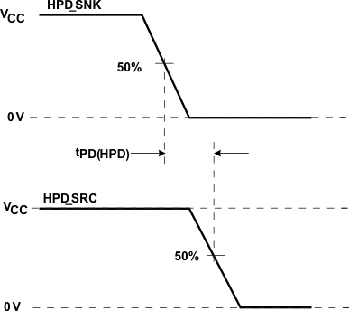 Figure 1. HPD Timing Diagram 1 Figure 1. HPD Timing Diagram 1
|
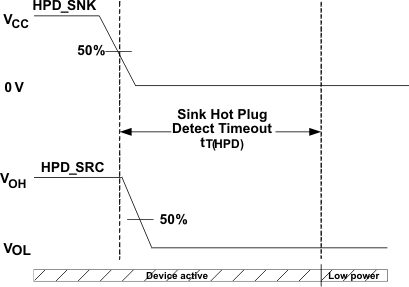 Figure 2. HPD Timing Diagram 2 Figure 2. HPD Timing Diagram 2
|
7.8 Typical Characteristics
Table 1. Characterization Test Board Trace Lengths Related to Input Jitter
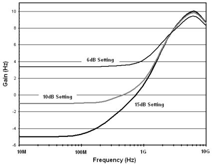
Gain represents SN75DP130 design simulation.
Figure 3. Typical EQ Gain Curves
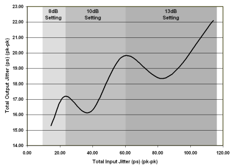
DisplayPort output jitter measured at the surface mount pins connected to the main link output channels on the SN75DP130 characterization test board; input jitter generated from test board with variable input trace lengths using 4 mil traces of lengths 2 inches to 22 inches generating the typical input jitter as represented in Table 1.
Figure 4. DisplayPort Sink Jitter Performance With Optimal EQ Settings
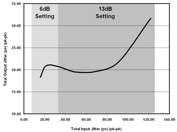
DisplayPort output jitter measured at the surface mount pins connected to the main link output channels on the SN75DP130 characterization test board; input jitter generated from test board with variable input trace lengths using 4 mil traces of lengths 2 inches to 22 inches generating the typical input jitter as represented in Table 1.
Figure 5. TMDS Sink jitter Performance With Optimal EQ Settings
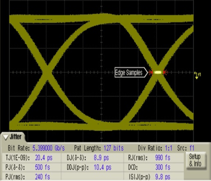 Figure 7. SN75DP130 Output; 10-Inch Input Trace; 13-dB EQ Setting; DP Sink
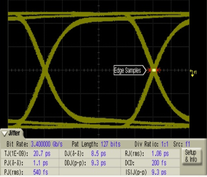 Figure 9. SN75DP130 Output; 10-Inch Input Trace; 13-dB EQ Setting; TMDS Sink
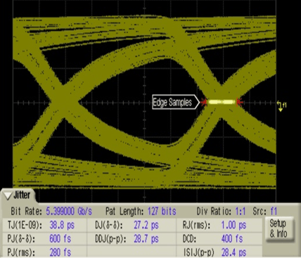
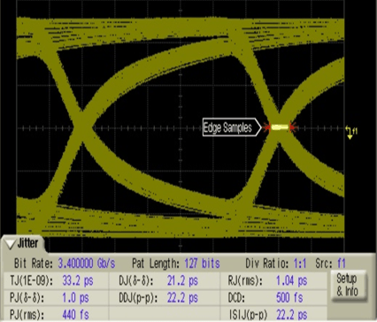 Figure 8. Main Link Input With 10-Inch Trace; TMDS Sink