SNLS692B December 2021 – December 2023 SN75LVPE5421
PRODUCTION DATA
- 1
- 1 Features
- 2 Applications
- 3 Description
- 4 Pin Configuration and Functions
- 5 Specifications
- 6 Detailed Description
- 7 Application and Implementation
- 8 Device and Documentation Support
- 9 Revision History
- 10Mechanical, Packaging, and Orderable Information
Package Options
Refer to the PDF data sheet for device specific package drawings
Mechanical Data (Package|Pins)
- RUA|42
Thermal pad, mechanical data (Package|Pins)
- RUA|42
Orderable Information
7.4.2 Layout Example
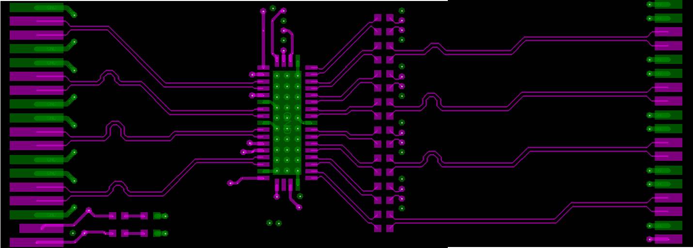
Figure 7-3 shows SN75LVPE5421 layout example.
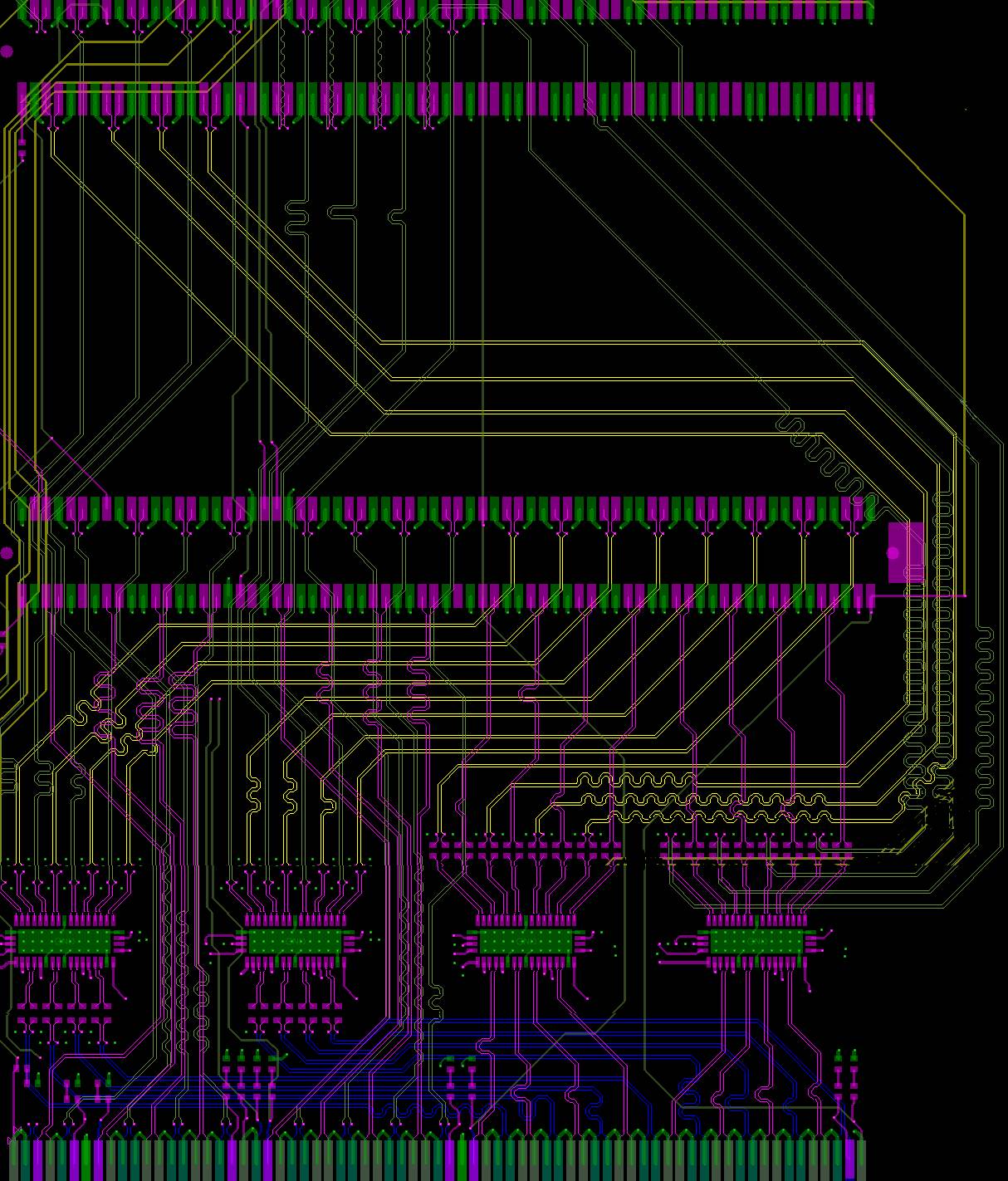
 Figure 7-3 SN75LVPE5421 Layout ExampleFigure 7-4 shows a layout illustration where two SN75LVPE5412 and two SN75LVPE5421 are used to switch 8 lanes between the two PCIe
slots.
 Figure 7-4 Layout Example for PCIe Lane Muxing
Application
 Figure 7-3 SN75LVPE5421 Layout Example
 Figure 7-4 Layout Example for PCIe Lane Muxing
Application