SLASF30A January 2022 – December 2024 TAA5212
PRODUCTION DATA
- 1
- 1 Features
- 2 Applications
- 3 Description
- 4 Pin Configuration and Functions
-
5 Specifications
- 5.1 Absolute Maximum Ratings
- 5.2 ESD Ratings
- 5.3 Recommended Operating Conditions
- 5.4 Thermal Information
- 5.5 Electrical Characteristics
- 5.6 Timing Requirements: I2C Interface
- 5.7 Switching Characteristics: I2C Interface
- 5.8 Timing Requirements: SPI Interface
- 5.9 Switching Characteristics: SPI Interface
- 5.10 Timing Requirements: TDM, I2S or LJ Interface
- 5.11 Switching Characteristics: TDM, I2S or LJ Interface
- 5.12 Timing Requirements: PDM Digital Microphone Interface
- 5.13 Switching Characteristics: PDM Digital Microphone Interface
- 5.14 Timing Diagrams
- 5.15 Typical Characteristics
-
6 Detailed Description
- 6.1 Overview
- 6.2 Functional Block Diagram
- 6.3
Feature Description
- 6.3.1 Serial Interfaces
- 6.3.2 Phase-Locked Loop (PLL) and Clock Generation
- 6.3.3 Input Channel Configurations
- 6.3.4 Reference Voltage
- 6.3.5 Programmable Microphone Bias
- 6.3.6
Signal-Chain Processing
- 6.3.6.1
ADC Signal-Chain
- 6.3.6.1.1 6 to 4 Input Select Multiplexer (6:4 MUX)
- 6.3.6.1.2 Programmable Channel Gain and Digital Volume Control
- 6.3.6.1.3 Programmable Channel Gain Calibration
- 6.3.6.1.4 Programmable Channel Phase Calibration
- 6.3.6.1.5 Programmable Digital High-Pass Filter
- 6.3.6.1.6 Programmable Digital Biquad Filters
- 6.3.6.1.7 Programmable Channel Summer and Digital Mixer
- 6.3.6.1.8
Configurable Digital Decimation Filters
- 6.3.6.1.8.1
Linear-phase filters
- 6.3.6.1.8.1.1 Sampling Rate: 8kHz or 7.35kHz
- 6.3.6.1.8.1.2 Sampling Rate: 16kHz or 14.7kHz
- 6.3.6.1.8.1.3 Sampling Rate: 24kHz or 22.05kHz
- 6.3.6.1.8.1.4 Sampling Rate: 32kHz or 29.4kHz
- 6.3.6.1.8.1.5 Sampling Rate: 48kHz or 44.1kHz
- 6.3.6.1.8.1.6 Sampling Rate: 96kHz or 88.2kHz
- 6.3.6.1.8.1.7 Sampling Rate: 192kHz or 176.4kHz
- 6.3.6.1.8.2 Low-latency Filters
- 6.3.6.1.8.3 Ultra Low-latency Filters
- 6.3.6.1.8.1
Linear-phase filters
- 6.3.6.1.9 Automatic Gain Controller (AGC)
- 6.3.6.1.10 Voice Activity Detection (VAD)
- 6.3.6.1.11 Ultrasonic Activity Detection (UAD)
- 6.3.6.1
ADC Signal-Chain
- 6.3.7 Digital PDM Microphone Record Channel
- 6.3.8 Interrupts, Status, and Digital I/O Pin Multiplexing
- 6.3.9 Power Tune Mode
- 6.3.10 Incremental ADC (IADC) Mode
- 6.4 Device Functional Modes
- 6.5 Programming
-
7 Register Maps
- 7.1 Device Configuration Registers
- 7.2
Programmable Coefficienct Registers
- 7.2.1 Programmable Coefficient Registers: Page 8
- 7.2.2 Programmable Coefficient Registers: Page 9
- 7.2.3 Programmable Coefficient Registers: Page 10
- 7.2.4 Programmable Coefficient Registers: Page 11
- 7.2.5 Programmable Coefficient Registers: Page 19
- 7.2.6 Programmable Coefficient Registers: Page 27
- 7.2.7 Programmable Coefficient Registers: Page 28
- 8 Application and Implementation
- 9 Device and Documentation Support
- 10Revision History
- 11Mechanical, Packaging, and Orderable Information
Package Options
Mechanical Data (Package|Pins)
- RGE|24
Thermal pad, mechanical data (Package|Pins)
- RGE|24
Orderable Information
6.3.6.1.9 Automatic Gain Controller (AGC)
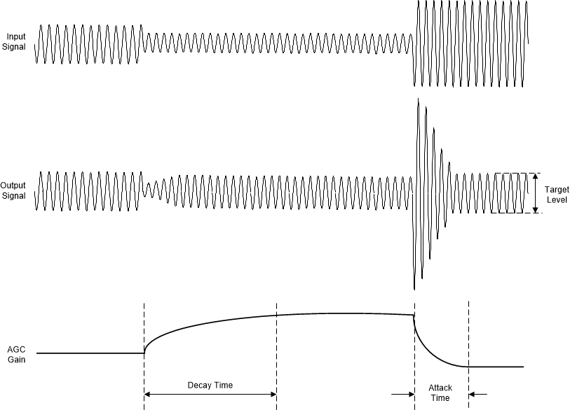
The device includes an automatic gain controller (AGC) for ADC recording. As shown in Figure 6-62, the AGC can be used to maintain a nominally constant output level when recording speech. Instead of manually setting the channel gain in AGC mode, the circuitry automatically adjusts the channel gain when the input signal becomes overly loud or very weak, such as when a person speaking into a microphone moves closer to or farther from the microphone. The AGC algorithm has several programmable parameters, including target level, maximum gain allowed, attack and release (or decay) time constants, and noise thresholds that allow the algorithm to be fine-tuned for any particular application. These are part of the programmable coefficients of the device for flexibility and can be configured using the registers in Section 7.2.6 and Section 7.2.7.
 Figure 6-62 AGC
Characteristics
Figure 6-62 AGC
CharacteristicsThe target level represents the nominal approximate output level at which the AGC attempts to hold the ADC output signal level. The TAA5212 allows programming of different target levels. The target level is recommended to be set with enough margin to prevent clipping when loud sounds occur. For further details on the AGC various configurable parameter and application use, see the Using the Automatic Gain Controller (AGC) in TAx5x1x Family application report. TI recommends using the PPC3 GUI for configuring the programmable coefficients settings; for more details see the TAC5212EVM-PDK Evaluation module user's guide and the PurePath™ console graphical development suite.