SLASEM6E october 2017 – july 2023 TAS2770
PRODUCTION DATA
- 1
- 1 Features
- 2 Applications
- 3 Description
- 4 Revision History
- 5 Pin Configuration and Functions
- 6 Specifications
- 7 Parameter Measurement Information
-
8 Detailed Description
- 8.1 Overview
- 8.2 Functional Block Diagram
- 8.3 Feature Description
- 8.4 Device Functional Modes
- 8.5
Register Maps
- 8.5.1 Register Summary Table Book=0x00 Page=0x00
- 8.5.2
Register Maps
- 8.5.2.1 PAGE (book=0x00 page=0x00 address=0x00) [reset=0h]
- 8.5.2.2 SW_RESET (book=0x00 page=0x00 address=0x01) [reset=0h]
- 8.5.2.3 PWR_CTL (book=0x00 page=0x00 address=0x02) [reset=Eh]
- 8.5.2.4 PB_CFG0 (book=0x00 page=0x00 address=0x03) [reset=10h]
- 8.5.2.5 PB_CFG1 (book=0x00 page=0x00 address=0x04) [reset=1h]
- 8.5.2.6 PB_CFG2 (book=0x00 page=0x00 address=0x05) [reset=0h]
- 8.5.2.7 PB_CFG3 (book=0x00 page=0x00 address=0x06) [reset=0h]
- 8.5.2.8 MISC_CFG (book=0x00 page=0x00 address=0x07) [reset=6h]
- 8.5.2.9 PDM_CFG0 (book=0x00 page=0x00 address=0x08) [reset=0h]
- 8.5.2.10 PDM_CFG1 (book=0x00 page=0x00 address=0x09) [reset=8h]
- 8.5.2.11 TDM_CFG0 (book=0x00 page=0x00 address=0x0A) [reset=7h]
- 8.5.2.12 TDM_CFG1 (book=0x00 page=0x00 address=0x0B) [reset=2h]
- 8.5.2.13 TDM_CFG2 (book=0x00 page=0x00 address=0x0C) [reset=Ah]
- 8.5.2.14 TDM_CFG3 (book=0x00 page=0x00 address=0x0D) [reset=10h]
- 8.5.2.15 TDM_CFG4 (book=0x00 page=0x00 address=0x0E) [reset=13h]
- 8.5.2.16 TDM_CFG5 (book=0x00 page=0x00 address=0x0F) [reset=2h]
- 8.5.2.17 TDM_CFG6 (book=0x00 page=0x00 address=0x10) [reset=0h]
- 8.5.2.18 TDM_CFG7 (book=0x00 page=0x00 address=0x11) [reset=4h]
- 8.5.2.19 TDM_CFG8 (book=0x00 page=0x00 address=0x12) [reset=6h]
- 8.5.2.20 TDM_CFG9 (book=0x00 page=0x00 address=0x13) [reset=7h]
- 8.5.2.21 TDM_CFG10 (book=0x00 page=0x00 address=0x14) [reset=8h]
- 8.5.2.22 LIM_CFG0 (book=0x00 page=0x00 address=0x15) [reset=14h]
- 8.5.2.23 LIM_CFG1 (book=0x00 page=0x00 address=0x16) [reset=76h]
- 8.5.2.24 LIM_CFG2 (book=0x00 page=0x00 address=0x17) [reset=10h]
- 8.5.2.25 LIM_CFG3 (book=0x00 page=0x00 address=0x18) [reset=6Eh]
- 8.5.2.26 LIM_CFG4 (book=0x00 page=0x00 address=0x19) [reset=1Eh]
- 8.5.2.27 LIM_CFG5 (book=0x00 page=0x00 address=0x1A) [reset=58h]
- 8.5.2.28 BOP_CFG0 (book=0x00 page=0x00 address=0x1B) [reset=1h]
- 8.5.2.29 BOP_CFG1 (book=0x00 page=0x00 address=0x1C) [reset=14h]
- 8.5.2.30 BOP_CFG2 (book=0x00 page=0x00 address=0x1D) [reset=4Eh]
- 8.5.2.31 ICLA_CFG0 (book=0x00 page=0x00 address=0x1E) [reset=0h]
- 8.5.2.32 ICLA_CFG1 (book=0x00 page=0x00 address=0x1F) [reset=0h]
- 8.5.2.33 INT_MASK0 (book=0x00 page=0x00 address=0x20) [reset=FCh]
- 8.5.2.34 INT_MASK1 (book=0x00 page=0x00 address=0x21) [reset=B1h]
- 8.5.2.35 INT_LIVE0 (book=0x00 page=0x00 address=0x22) [reset=0h]
- 8.5.2.36 INT_LIVE1 (book=0x00 page=0x00 address=0x23) [reset=0h]
- 8.5.2.37 INT_LTCH0 (book=0x00 page=0x00 address=0x24) [reset=0h]
- 8.5.2.38 INT_LTCH1 (book=0x00 page=0x00 address=0x25) [reset=0h]
- 8.5.2.39 INT_LTCH2 (book=0x00 page=0x00 address=0x26) [reset=0h]
- 8.5.2.40 VBAT_MSB (book=0x00 page=0x00 address=0x27) [reset=0h]
- 8.5.2.41 VBAT_LSB (book=0x00 page=0x00 address=0x28) [reset=0h]
- 8.5.2.42 TEMP_MSB (book=0x00 page=0x00 address=0x29) [reset=0h]
- 8.5.2.43 TEMP_LSB (book=0x00 page=0x00 address=0x2A) [reset=0h]
- 8.5.2.44 INT_CFG (book=0x00 page=0x00 address=0x30) [reset=5h]
- 8.5.2.45 DIN_PD (book=0x00 page=0x00 address=0x31) [reset=0h]
- 8.5.2.46 MISC_IRQ (book=0x00 page=0x00 address=0x32) [reset=81h]
- 8.5.2.47 CLOCK_CFG (book=0x00 page=0x00 address=0x3C) [reset=Dh]
- 8.5.2.48 TDM_DET (book=0x00 page=0x00 address=0x77) [reset=7Fh]
- 8.5.2.49 REV_ID (book=0x00 page=0x00 address=0x7D) [reset=20h]
- 8.5.2.50 I2C_CKSUM (book=0x00 page=0x00 address=0x7E) [reset=0h]
- 8.5.2.51 BOOK (book=0x00 page=0x00 address=0x7F) [reset=0h]
-
9 Application and Implementation
- 9.1 Application Information
- 9.2 Typical Application
- 9.3
Initialization Set Up
- 9.3.1 Initial Device Configuration - Auto Rate
- 9.3.2 Initial Device Configuration - 48 kHz
- 9.3.3 Initial Device Configuration - 44.1 kHz
- 9.3.4 Sample Rate Change - 48 kHz to 44.1kHz
- 9.3.5 Sample Rate Change - 44.1 kHz to 48 kHz
- 9.3.6 Device Mute
- 9.3.7 Device Un-Mute
- 9.3.8 Device Sleep
- 9.3.9 Device Wake
- 10Power Supply Recommendations
- 11Layout
- 12Device and Documentation Support
- 13Mechanical, Packaging, and Orderable Information
Package Options
Mechanical Data (Package|Pins)
Thermal pad, mechanical data (Package|Pins)
Orderable Information
8.4.5 IV Sense
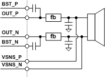
The TAS2770 provides speaker voltage and current sense for real time monitoring of loudspeaker behavior. The VSNS_P and VSNS_N pins should be connected after any ferrite bead filter (or directly to the OUT_P and OUT_N connections if no EMI filter is used). The V-Sense connections eliminate IR drop error due to packaging, PCB interconnect or ferrite bead filter resistance. It should be noted that any interconnect resistance after the V-Sense terminals will not be corrected for, so it is advised to connect the sense connections as close to the load as possible.
 Figure 8-17 V-Sense Connections
I-Sense and V-Sense can be powered down by asserting the ISNS_PD and VSNS_PD register bits respectively. When powered down, the device will return null samples for the powered down block.
| ISNS_PD | Setting |
|---|---|
| I-Sense is active (default) |
| I-Sense is powered down |
| VSNS_PD | Setting |
|---|---|
| V-Sense is active (default) |
| V-Sense is powered down |