SLOS836E May 2013 – June 2016 TAS5729MD
PRODUCTION DATA.
- 1 Features
- 2 Applications
- 3 Description
- 4 Revision History
- 5 Related Devices
- 6 Pin Configuration and Functions
-
7 Specifications
- 7.1 Absolute Maximum Ratings
- 7.2 ESD Ratings
- 7.3 Recommended Operating Conditions
- 7.4 Thermal Information
- 7.5 Digital I/O Pins
- 7.6 Master Clock
- 7.7 Serial Audio Port
- 7.8 Protection Circuitry
- 7.9 Speaker Amplifier in All Modes
- 7.10 Speaker Amplifier in Stereo Bridge Tied Load (BTL) Mode
- 7.11 Speaker Amplifier in Stereo Post-Filter Parallel Bridge Tied Load (Post-Filter PBTL) Mode
- 7.12 Headphone Amplifier and Line Driver
- 7.13 Reset Timing
- 7.14 I2C Control Port
- 7.15 Typical Electrical Power Consumption
- 7.16 Typical Characteristics
- 8 Parameter Measurement Information
-
9 Detailed Description
- 9.1 Overview
- 9.2 Functional Block Diagram
- 9.3 Feature Description
- 9.4 Device Functional Modes
- 9.5 Programming
- 9.6
Register Maps
- 9.6.1 Clock Control Register (0x00)
- 9.6.2 Device ID Register (0x01)
- 9.6.3 Error Status Register (0x02)
- 9.6.4 System Control Register 1 (0x03)
- 9.6.5 Serial Data Interface Register (0x04)
- 9.6.6 System Control Register 2 (0x05)
- 9.6.7 Soft Mute Register (0x06)
- 9.6.8 Volume Registers (0x07, 0x08, 0x09)
- 9.6.9 Volume Configuration Register (0x0E)
- 9.6.10 Modulation Limit Register (0x10)
- 9.6.11 Interchannel Delay Registers (0x11, 0x12, 0x13, and 0x14)
- 9.6.12 PWM Shutdown Group Register (0x19)
- 9.6.13 Start/Stop Period Register (0x1A)
- 9.6.14 Oscillator Trim Register (0x1B)
- 9.6.15 BKND_ERR Register (0x1C)
- 9.6.16 Input Multiplexer Register (0x20)
- 9.6.17 Channel 4 Source Select Register (0x21)
- 9.6.18 PWM Output MUX Register (0x25)
- 9.6.19 AGL Control Register (0x46)
- 9.6.20 PWM Switching Rate Control Register (0x4F)
- 9.6.21 EQ Control (0x50)
-
10Application and Implementation
- 10.1 Application Information
- 10.2
Typical Applications
- 10.2.1 Stereo BTL Configuration With Headphone and Line Driver Amplifier
- 10.2.2 Mono PBTL Configuration with Headphone and Line Driver Amplifier
- 11Power Supply Recommendations
- 12Layout
- 13Device and Documentation Support
- 14Mechanical, Packaging, and Orderable Information
Package Options
Mechanical Data (Package|Pins)
- DCA|48
Thermal pad, mechanical data (Package|Pins)
- DCA|48
Orderable Information
7 Specifications
7.1 Absolute Maximum Ratings(1)
Over operating free-air temperature range (unless otherwise noted).| MIN | MAX | UNIT | ||
|---|---|---|---|---|
| Temperature | Ambient operating temperature, TA | 0 | 85 | °C |
| Supply voltage | DVDD, DRVDD, AVDD | –0.3 | 4.2 | V |
| PVDD | –0.3 | 30 | V | |
| Input voltage | DVDD referenced digital inputs | –0.5 | DVDD + 0.5 | V |
| 5-V tolerant digital inputs (2) | –0.5 | DVDD + 2.5(3) | V | |
| DR_INx | DRVSS – 0.3 | DRVDD + 0.3 | V | |
| HP Load | RLOAD(HP) | 12.8 | N/A | Ω |
| Line Driver Load | RLOAD(LD) | 600 | N/A | Ω |
| Voltage at speaker output pins | SPK_OUTx | –0.03 | 32 | V |
| Voltage at BSTRPx pins | BSTRPx | –0.03 | 39 | V |
| Storage temperature, Tstg | –40 | 125 | °C | |
(1) Stresses beyond those listed under Absolute Maximum Ratings can cause permanent damage to the device. These are stress ratings only, and functional operation of the device at these or any other conditions beyond those indicated under Recommended Operating Conditions is not implied. Exposure to absolute-maximum-rated conditions for extended periods can affect device reliability.
(2) 5-V tolerant inputs are PDN, RESET, SCLK, LRCLK, MCLK, SDIN, SDA, and SCL.
(3) Maximum pin voltage should not exceed 6 V.
7.2 ESD Ratings
| VALUE | UNIT | |||
|---|---|---|---|---|
| V(ESD) | Electrostatic discharge | Human-body model (HBM), per ANSI/ESDA/JEDEC JS-001(1) | ±1000 | V |
| Charged-device model (CDM), per JEDEC specification JESD22-C101(2) | ±250 | |||
(1) JEDEC document JEP155 states that 500-V HBM allows safe manufacturing with a standard ESD control process.
(2) JEDEC document JEP157 states that 250-V CDM allows safe manufacturing with a standard ESD control process.
7.3 Recommended Operating Conditions
over operating free-air temperature range (unless otherwise noted)| MIN | MAX | UNIT | ||
|---|---|---|---|---|
| TA | Ambient operating temperature | 0 | 85 | °C |
| VDD | DVDD, DRVDD, and AVDD supply | 2.97 | 3.63 | V |
| PVDD | PVDD supply | 4.5 | 26.4(1) | V |
| VIH | Input logic high | 2 | V | |
| VIL | Input logic low | 0.8 | V | |
| RHP | Minimum HP load | 16 | Ω | |
| RLD | Minimum line driver load | 600 | Ω | |
| RSPK(BTL) | Minimum speaker load in BTL mode | 4 | Ω | |
| RSPK(PBTL) | Minimum speaker load in post-filter PBTL mode | 4 | Ω | |
| LFILT | Minimum output inductance under short-circuit condition | 10 | µH | |
(1) For operation at PVDD levels greater than 18 V, the modulation limit must be set to 93.8% via the control port register 0x10.
7.4 Thermal Information
| THERMAL METRIC(1) | TAS5729MD | UNIT | ||
|---|---|---|---|---|
| DCA(2) | DCA(3) | |||
| 48 PINS | ||||
| RθJA | Junction-to-ambient thermal resistance | 62.6 | 32.6 | °C/W |
| RθJC(top) | Junction-to-case (bottom) thermal resistance | 17.9 | 16.2 | °C/W |
| RθJB | Junction-to-board thermal resistance | 11.9 | 14.4 | °C/W |
| ψJT | Junction-to-top characterization parameter | 0.8 | 0.9 | °C/W |
| ψJB | Junction-to-board characterization parameter | 13.5 | 14.3 | °C/W |
| RθJC(bottom) | Junction-to-case (top) thermal resistance | 1.5 | 1.4 | °C/W |
(1) For more information about traditional and new thermal metrics, see the Semiconductor and IC Package Thermal Metricsapplication report.
(2) JEDEC Standard 2 Layer Board
(3) JEDEC Standard 4 Layer Board
7.5 Digital I/O Pins
over operating free-air temperature range (unless otherwise noted)| PARAMETER | TEST CONDITIONS | MIN | TYP | MAX | UNIT | |
|---|---|---|---|---|---|---|
| |IIH| | Input logic high current level | All digital pins | 75 | µA | ||
| VIH | Input logic high threshold for DVDD referenced digital inputs | All digital pins | 2 | V | ||
| |IIL| | Input logic low current level | All digital pins | 75 | µA | ||
| VIL | Input logic low threshold for DVDD referenced digital inputs | All digital pins | 0.8 | V | ||
| VOH | Output logic high voltage level | IOH = 4 mA, VDD = 3 V | 2.4 | V | ||
| VOL | Output logic low voltage level | IOH = –4 mA, VDD = 3 V | 0.5 | V | ||
7.6 Master Clock
over operating free-air temperature range (unless otherwise noted)| PARAMETER | MIN | TYP | MAX | UNIT | |
|---|---|---|---|---|---|
| DMCLK | Allowable MCLK duty cycle | 40% | 50% | 60% | |
| fMCLK | Supported MCLK frequencies | 2.8224 | 24.576 | MHz | |
| tr
tf |
Rise or fall time for MCLK | 5 | ns | ||
7.7 Serial Audio Port
over operating free-air temperature range (unless otherwise noted)| PARAMETER | TEST CONDITIONS | MIN | TYP | MAX | UNIT | |
|---|---|---|---|---|---|---|
| fSCLK | Supported SCLK frequencies | Values include 32, 48, and 64 | 32 | 64 | × fS | |
| DSCLK | Allowable SCLK duty cycle | 40% | 50% | 60% | ||
| tsu2 | Required SDIN setup time before SCLK rising edge | 10 | ns | |||
| th2 | Required SDIN hold time after SCLK rising edge | 10 | ns | |||
| fS | Supported input sample rates | 8 | 48 | kHz | ||
| DLRCLK | Allowable LRCLK duty cycle | 40% | 50% | 60% | ||
| tsu1 | Required LRCLK to SCLK rising edge 10 | ns | ||||
| th1 | Required LRCLK to SCLK rising edge | 10 | ns | |||
| tr, tf | Rise or fall time for SCLK and LRCLK | 8 | ns | |||
| Allowable LRCLK drift before LRCLK reset | 4 | MCLKs | ||||
7.8 Protection Circuitry
over operating free-air temperature range (unless otherwise noted)| PARAMETER | TEST CONDITIONS | MIN | TYP | MAX | UNIT | |
|---|---|---|---|---|---|---|
| OCETHRES | Overcurrent threshold for each BTL output | PVDD = 15 V, TA = 25°C | 4.5 | A | ||
| UVETHRES(PVDD) | Undervoltage error (UVE) threshold | PVDD falling | 4 | V | ||
| UVETHRES(AVDD) | Undervoltage error (UVE) threshold | AVDD falling | 4.1 | V | ||
| UVEHYST(PVDD) | UVE recovery threshold | PVDD rising | 4.5 | V | ||
| UVEHYST(AVDD) | UVE recovery threshold | AVDD rising | 2.7 | V | ||
| OTETHRES | Overtemperature error (OTE) threshold | 150 | °C | |||
| OTEHYST | OTE recovery threshold | 30 | °C | |||
7.9 Speaker Amplifier in All Modes
over operating free-air temperature range (unless otherwise noted)| PARAMETER | TEST CONDITIONS | MIN | TYP | MAX | UNIT | |
|---|---|---|---|---|---|---|
| fSPK_AMP | Speaker amplifier switching frequency | 11.025-, 22.05-, or 44.1-kHz data rate ±2% | 352.8 | kHz | ||
| 48-, 24-, 12-, 8-, 16-, or 32-kHz data rate ±2% | 384 | kHz | ||||
| RDS(ON) | On resistance of output MOSFET (both high-side and low-side) | PVDD = 15 V, TA = 25°C, die only | 200 | mΩ | ||
| PVDD = 15 V, TA = 25°C, includes: die, bond wires, leadframe |
240 | mΩ | ||||
| RPD | Internal pulldown resistor at output of each half-bridge making up the full bridge outputs | Connected when drivers are hi-Z to provide bootstrap capacitor charge | 3 | kΩ | ||
7.10 Speaker Amplifier in Stereo Bridge Tied Load (BTL) Mode
TA = 25°C, PVDD = 18 V, AVDD = DRVDD = DVDD = 3.3 V, audio input signal = 1-kHz sine wave, BTL, AD mode, fS = 48 kHz, RSPK = 8 Ω, AES17 filter, fPWM = 384 kHz, external components per Typical Characteristics, and in accordance with recommended operating conditions (unless otherwise specified).| PARAMETER | TEST CONDITIONS | MIN | TYP | MAX | UNIT | |
|---|---|---|---|---|---|---|
| ICN(SPK) | Idle channel noise | PVDD = 18 V, A-Weighted | 56 | µVrms | ||
| PO(SPK) | Maximum continuous output power per channel | PVDD = 13 V, 10% THD, 1-kHz input signal | 10.5 | W | ||
| PVDD = 8 V, 10% THD, 1-kHz input signal | 4 | W | ||||
| PVDD = 18 V, 10% THD, 1-kHz input signal | 12 | W | ||||
| SNR(SPK) | Signal-to-noise ratio (referenced to 0dBFS input signal) | PVDD = 18 V, A-weighted, f = 1 kHz, maximum power at THD < 1% | 105 | dB | ||
| THD+N(SPK) | Total harmonic distortion and noise | PVDD = 18 V; PO = 1 W | 0.15% | |||
| PVDD = 13 V; PO = 1 W | 0.13% | |||||
| PVDD = 8 V; PO = 1 W | 0.2% | |||||
| X-Talk(SPK) | Crosstalk (worst case between L-to-R and R-to-L coupling) | PO = 1 W, f = 1 kHz (BD mode) | –70 | dB | ||
| PO = 1 W, f = 1 kHz (AD mode) | –48 | dB | ||||
7.11 Speaker Amplifier in Stereo Post-Filter Parallel Bridge Tied Load (Post-Filter PBTL) Mode
TA = 25°C, PVDD = 18 V, AVDD = DRVDD = DVDD = 3.3 V, audio input signal = 1-kHz sine wave, BTL, AD mode, fS = 48 kHz, RSPK = 4 Ω, AES17 filter, fPWM = 384 kHz, external components per Typical Characteristics, and in accordance with recommended operating conditions (unless otherwise specified).| PARAMETER | TEST CONDITIONS | MIN | TYP | MAX | UNIT | |
|---|---|---|---|---|---|---|
| ICN(SPK) | Idle channel noise | PVDD = 18 V, A-Weighted | 42 | µVrms | ||
| PO(SPK) | Maximum continuous output power per channel | PVDD = 13 V, 10% THD, 1-kHz input signal | 18.9 | W | ||
| PVDD = 8 V, 10% THD, 1-kHz input signal | 7.2 | W | ||||
| PVDD = 18 V, 10% THD, 1-kHz input signal | 24 | W | ||||
| SNR(SPK) | Signal-to-noise ratio (referenced to 0dBFS input signal) | PVDD = 18 V, A-weighted, f = 1 kHz, maximum power at THD < 1% | 105 | dB | ||
| THD+N(SPK) | Total harmonic distortion and noise | PVDD = 18 V; PO = 1 W | 0.06% | |||
| PVDD = 13 V; PO = 1 W | 0.03% | |||||
| PVDD = 8 V; PO = 1 W | 0.15% | |||||
7.12 Headphone Amplifier and Line Driver
over operating free-air temperature range (unless otherwise noted)| PARAMETER | TEST CONDITIONS | MIN | TYP | MAX | UNIT | |
|---|---|---|---|---|---|---|
| fCP | Charge pump switching frequency | 200 | 300 | 400 | kHz | |
| PO(HP) | Headphone amplifier output power | RLOAD(HP) = 32 Ω, THD+N = 1%, outputs in phase | 55 | mW | ||
| SNR(HP) | Signal-to-noise ratio | (Referenced to 55-mW output signal), RLOAD(HP) = 32 Ω, A-Weighted | 101 | dB | ||
| SNR(LD) | Signal-to-noise ratio | (Referenced to 2-Vrms output signal), RLOAD(LD) = 10 kΩ, A-Weighted | 105 | dB | ||
7.13 Reset Timing
over operating free-air temperature range (unless otherwise noted)| MIN | NOM | MAX | UNIT | ||
|---|---|---|---|---|---|
| tw(RESET) | Pulse duration required to reset the device | 100 | µs | ||
7.14 I2C Control Port
over operating free-air temperature range (unless otherwise noted)| PARAMETER | TEST CONDITIONS | MIN | TYP | MAX | UNIT | |
|---|---|---|---|---|---|---|
| CL(I²C) | Allowable load capacitance for each I2C line | 400 | pF | |||
| fSCL | Supported SCL frequency | No wait states | 100 | 400 | kHz | |
| tbuf | Bus free time between stop and start conditions | 1.3 | µs | |||
| tf(I²C) | Rise time, SCL and SDA | 300 | ns | |||
| th1(I²C) | Hold time, SCL to SDA | 0 | ns | |||
| th2(I²C) | Hold time, start condition to SCL | 0.6 | µs | |||
| tI²C(start) | I2C startup time | Time to enable I2C from RST release | 12 | ms | ||
| tr(I²C) | Rise time, SCL and SDA | 300 | ns | |||
| tsu1(I²C) | Setup time, SDA to SCL | 100 | ns | |||
| tsu2(I²C) | Setup time, SCL to start condition | 0.6 | µs | |||
| tsu3(I²C) | Setup time, SCL to stop condition | 0.6 | µs | |||
| Tw(H) | Required pulse duration, SCL high | 0.6 | µs | |||
| Tw(L) | Required pulse duration, SCL low | 1.3 | µs | |||
 Figure 1. SCL and SDA Timing for I2C Control Port
 Figure 2. Start and Stop Timing Conditions
7.15 Typical Electrical Power Consumption
over operating free-air temperature range (unless otherwise noted), with DVDD = DRVDD = 3.3 V and AVDD = PVDD, external components as specified on the EVM.| SPEAKER AMPLIFIER STATE | CONFIGURATION SETTINGS | VPVDD
[V] |
IPVDD
[mA] |
IVDD
[mA] |
PDISS
(From all Supplies) [W] |
|
|---|---|---|---|---|---|---|
| fSPK_AMP | OPERATIONAL STATE | |||||
| 384kHz | Idle | RST pulled high, speaker amplifier outputs at 50/50 mute | 18 | 20 | 48 | 0.51 |
| Reset | RST pulled low, PDN pulled high | 5 | 21 | 0.16 | ||
7.16 Typical Characteristics
7.16.1 Speaker Amplifier
 Figure 5. Total Harmonic Distortion + Noise vs Frequency in BTL Mode With PVDD = 12 V
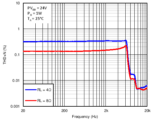 Figure 7. Total Harmonic Distortion + Noise vs Frequency in BTL Mode With PVDD = 24 V
 Figure 9. Total Harmonic Distortion + Noise vs Frequency in Post-Filter PBTL Mode With PVDD = 18 V
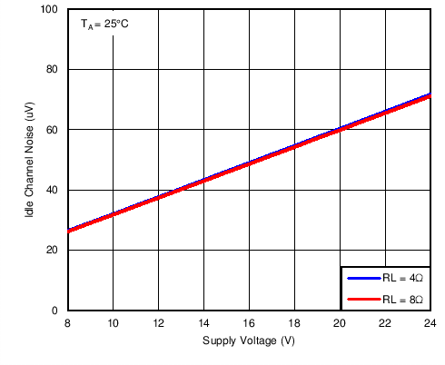 Figure 11. Stereo BTL Idle Channel Noise vs PVDD
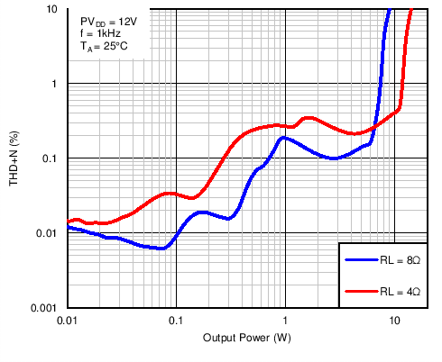 Figure 13. Total Harmonic Distortion + Noise vs Output Power in BTL Mode With PVDD = 12 V
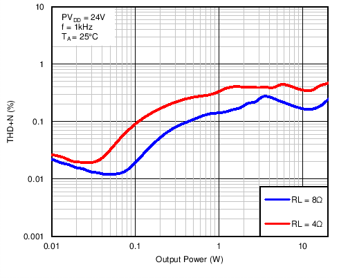 Figure 15. Total Harmonic Distortion + Noise vs Output Power in BTL Mode With PVDD = 24 V
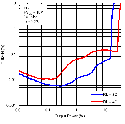 Figure 17. Total Harmonic Distortion + Noise vs Output Power in Post-Filter PBTL Mode With PVDD = 18 V
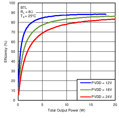
All channels driven
Figure 19. Efficiency vs Output Power in BTL Mode
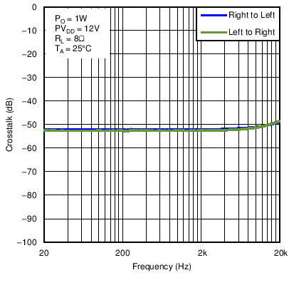 Figure 21. 8-Ohm Load Crosstalk vs Frequency in BTL Mode With PVDD = 12 V
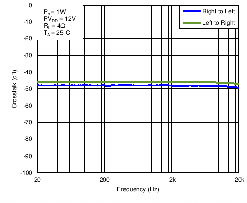 Figure 23. 4-Ohm Load Crosstalk vs Frequency in BTL Mode With PVDD = 12 V
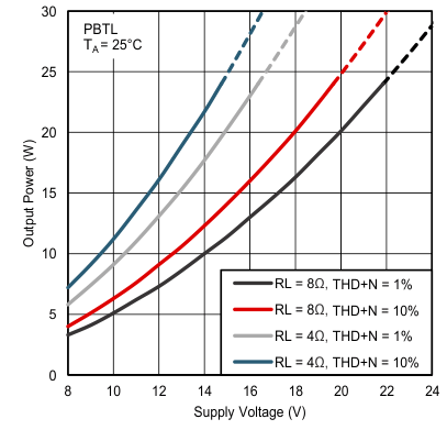
NOTE:
Dashed lines represent thermally limited region.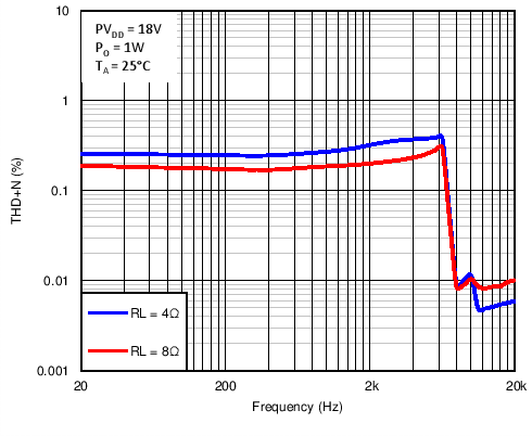 Figure 6. Total Harmonic Distortion + Noise vs Frequency in BTL Mode With PVDD = 18 V
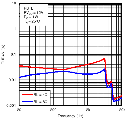 Figure 8. Total Harmonic Distortion + Noise vs Frequency in Post-Filter PBTL Mode With PVDD = 12 V
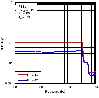 Figure 10. Total Harmonic Distortion + Noise vs Frequency in Post-Filter PBTL Mode With PVDD = 24 V
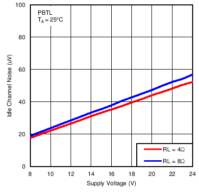 Figure 12. Post-Filter PBTL Idle Channel Noise vs PVDD
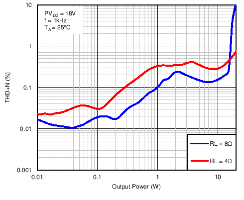 Figure 14. Total Harmonic Distortion + Noise vs Output Power in BTL Mode With PVDD = 18 V
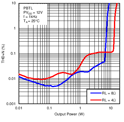 Figure 16. Total Harmonic Distortion + Noise vs Output Power in Post-Filter PBTL Mode With PVDD = 12 V
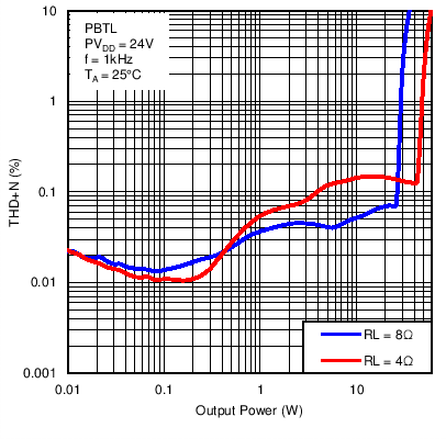 Figure 18. Total Harmonic Distortion + Noise vs Output Power in Post-Filter PBTL Mode With PVDD = 24 V
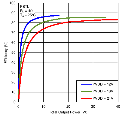
All channels driven
Figure 20. Efficiency vs Output Power in Post-Filter PBTL Mode
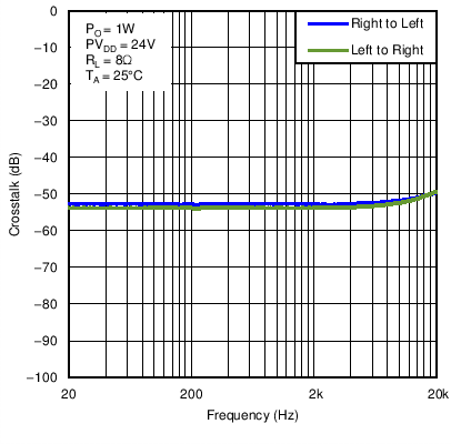 Figure 22. 8-Ohm Load Crosstalk vs Frequency in BTL Mode With PVDD = 24 V
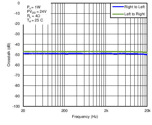 Figure 24. 4-Ohm Load Crosstalk vs Frequency in BTL Mode With PVDD = 24 V
7.16.2 Headphone Amplifier
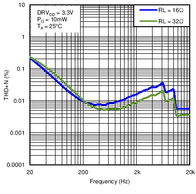 Figure 25. Headphone Total Harmonic Distortion + Noise vs Frequency With DRVDD = 3.3 V
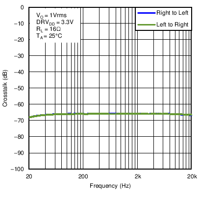 Figure 27. Headphone Crosstalk vs Frequency with DRVDD = 3.3 V and RHP = 16 Ω
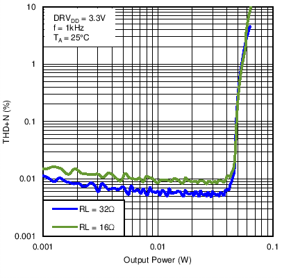 Figure 26. Headphone Total Harmonic Distortion + Noise vs Output Power With DRVDD = 3.3 V
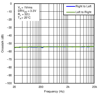 Figure 28. Headphone Crosstalk vs Frequency with DRVDD = 3.3 V and RHP = 32 Ω
7.16.3 Line Driver
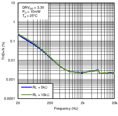 Figure 29. Line Driver Total Harmonic Distortion + Noise vs Frequency With DRVDD = 3.3 V
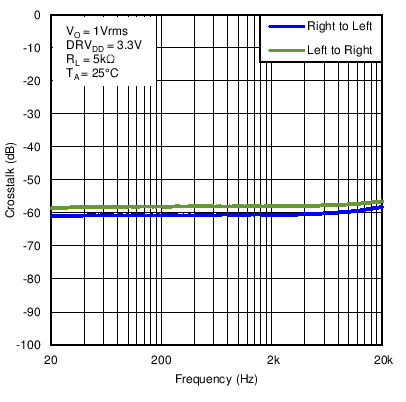 Figure 31. Line Driver Crosstalk vs Frequency With DRVDD = 3.3 V
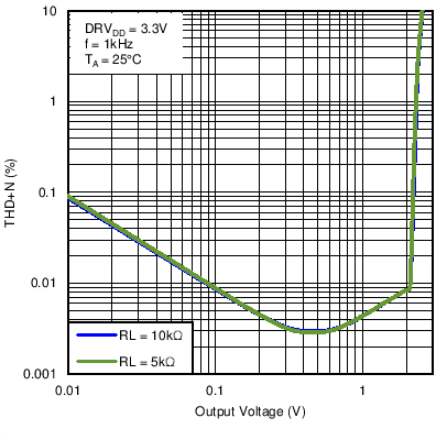 Figure 30. Line Driver THD+N vs Output Voltage With DRVDD = 3.3 V
