SLOS982C August 2017 – April 2018 TAS5755M
PRODUCTION DATA.
- 1 Features
- 2 Applications
- 3 Description
- 4 Revision History
- 5 Device Comparison Table
- 6 Pin Configuration and Functions
-
7 Specifications
- 7.1 Absolute Maximum Ratings
- 7.2 ESD Ratings
- 7.3 Recommended Operating Conditions
- 7.4 Thermal Information
- 7.5 PWM Operation at Recommended Operating Conditions
- 7.6 DC Electrical Characteristics
- 7.7 AC Electrical Characteristics (BTL, PBTL)
- 7.8 Electrical Characteristics - PLL External Filter Components
- 7.9 Electrical Characteristic - I2C Serial Control Port Operation
- 7.10 Timing Requirements - PLL Input Parameters
- 7.11 Timing Requirements - Serial Audio Ports Slave Mode
- 7.12 Timing Requirements - I2C Serial Control Port Operation
- 7.13 Timing Requirements - Reset (RESET)
- 7.14 Typical Characteristics
- 8 Parameter Measurement Information
-
9 Detailed Description
- 9.1 Overview
- 9.2 Functional Block Diagrams
- 9.3
Feature Description
- 9.3.1 Power Supply
- 9.3.2 I2C Address Selection and Fault Output
- 9.3.3 Single-Filter PBTL Mode
- 9.3.4 Device Protection System
- 9.3.5 SSTIMER Functionality
- 9.3.6 Clock, Autodetection, and PLL
- 9.3.7 PWM Section
- 9.3.8 2.1-Mode Support
- 9.3.9 I2C Compatible Serial Control Interface
- 9.3.10 Audio Serial Interface
- 9.3.11 Dynamic Range Control (DRC)
- 9.4 Device Functional Modes
- 9.5 Programming
- 9.6
Register Maps
- 9.6.1 Register Map Summary
- 9.6.2
Register Maps
- 9.6.2.1 Clock Control Register (0x00)
- 9.6.2.2 Device ID Register (0x01)
- 9.6.2.3 Error Status Register (0x02)
- 9.6.2.4 System Control Register 1 (0x03)
- 9.6.2.5 Serial Data Interface Register (0x04)
- 9.6.2.6 System Control Register 2 (0x05)
- 9.6.2.7 Soft Mute Register (0x06)
- 9.6.2.8 Volume Registers (0x07, 0x08, 0x09, 0x0A)
- 9.6.2.9 Volume Configuration Register (0x0E)
- 9.6.2.10 Modulation Limit Register (0x10)
- 9.6.2.11 Interchannel Delay Registers (0x11, 0x12, 0x13, and 0x14)
- 9.6.2.12 PWM Shutdown Group Register (0x19)
- 9.6.2.13 Start/Stop Period Register (0x1A)
- 9.6.2.14 Oscillator Trim Register (0x1B)
- 9.6.2.15 BKND_ERR Register (0x1C)
- 9.6.2.16 Input Multiplexer Register (0x20)
- 9.6.2.17 Channel 4 Source Select Register (0x21)
- 9.6.2.18 PWM Output Mux Register (0x25)
- 9.6.2.19 DRC Control Register (0x46)
- 9.6.2.20 Bank Switch and EQ Control Register (0x50)
-
10Application and Implementation
- 10.1 Application Information
- 10.2
Typical Applications
- 10.2.1 Stereo Bridge Tied Load Application
- 10.2.2 Mono Parallel Bridge Tied Load Application
- 10.2.3 2.1 Application
- 11Power Supply Recommendations
- 12Layout
- 13Device and Documentation Support
Package Options
Mechanical Data (Package|Pins)
- DFD|56
Thermal pad, mechanical data (Package|Pins)
- DFD|56
Orderable Information
7.14.3 Typical Characteristics, PBTL Configuration
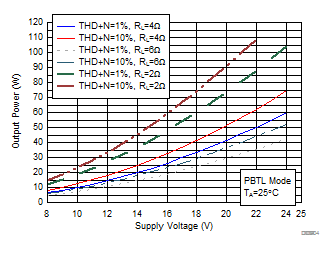 Figure 32. Output Power vs Supply Voltage
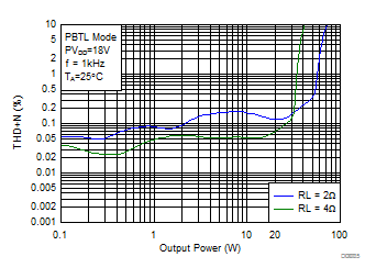 Figure 34. Total Harmonic Distortion + Noise vs Output Power (PBTL Mode)
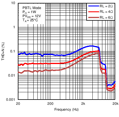 Figure 36. Total Harmonic Distortion vs Frequency (PBTL Mode)
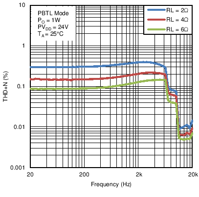 Figure 38. Total Harmonic Distortion vs Frequency (PBTL Mode)
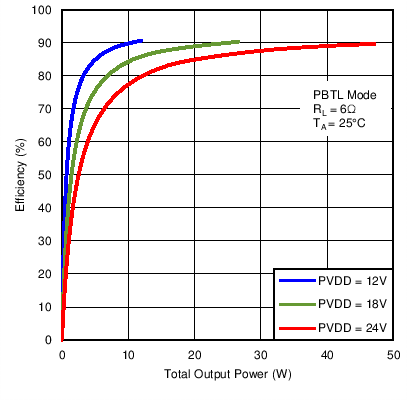 Figure 40. Efficiency vs Output Power (PBTL Mode)
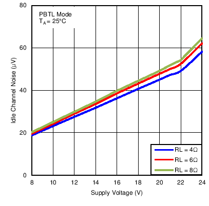 Figure 42. Idle Channel Noise vs Supply Voltage (PBTL Mode)
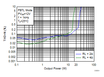
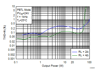 Figure 35. Total Harmonic Distortion + Noise vs Output Power (PBTL Mode)
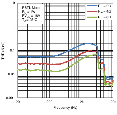 Figure 37. Total Harmonic Distortion vs Frequency (PBTL Mode)
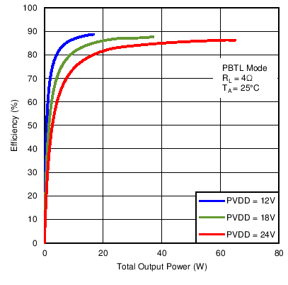 Figure 39. Efficiency vs Output Power (PBTL Mode)
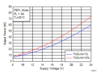 Figure 41. Power vs Supply Voltage (PBTL Mode)
